Service Manuals, User Guides, Schematic Diagrams or docs for : . Electronic Components Datasheets Active components Transistors KEC ktb1423

<< Back | Home

Most service manuals and schematics are PDF files, so You will need Adobre Acrobat Reader to view : Acrobat Download Some of the files are DjVu format. Readers and resources available here : DjVu Resources
For the compressed files, most common are zip and rar. Please, extract files with Your favorite compression software ( WinZip, WinRAR ... ) before viewing. If a document has multiple parts, You should download all, before extracting.
Good luck. Repair on Your own risk. Make sure You know what You are doing.


Image preview - the first page of the document
ktb1423


>> Download ktb1423 documenatation <<

Text preview - extract from the document
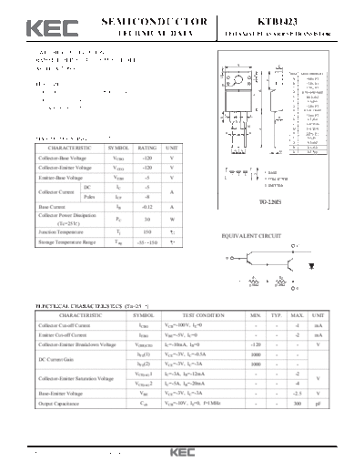
                                    SEMICONDUCTOR                                                                                   KTB1423
                                              TECHNICAL DATA                                   EPITAXIAL PLANAR PNP TRANSISTOR


  SWITCHING APPLICATIONS.
  HAMMER DRIVER, PULSE MOTOR DRIVER
                                                                                                           A                                      C
  APPLICATIONS.
                                                                                                                                                       DIM       MILLIMETERS


                                                                                                                               F
                                                                                       S
                                                                                                                                                        A                 _
                                                                                                                                                                    10.0 + 0.3


                                                                                                                                         P
                                                                                                                                                                          _
  FEATURES                                                                                 E                                                            B
                                                                                                                                                        C
                                                                                                                                                                    15.0 + 0.3
                                                                                                                                                                          _
                                                                                                                                                                    2.70 + 0.3


                                                                                                                                    B
    High DC Current Gain : hFE=1000(Min.) at VCE=-3V, IC=-3A.                                                                                           D        0.76+0.09/-0.05


                                                                                                                               G
                                                                                                                                                        E           3.2 + 0.2
                                                                                                                                                                          _
    High Collector Breakdown Voltage : VCEO=-120V (Min.)                                                                                                F                _
                                                                                                                                                                     3.0 + 0.3
                                                                                                                                                       G                  _
                                                                                                                                                                    12.0 + 0.3
    Complementary to KTD1413.                                                                                                                          H          0.5+0.1/-0.05
                                                                                               L                           L                           J                  _
                                                                                                                                                                    13.6 + 0.5


                                                                                       K
                                                                                                                                                  R                      _
                                                                                                                                                       K             3.7 + 0.2
                                                                                                                                                       L          1.2+0.25/-0.1
                                                                                                                       M
                                                                                                                                                       M          1.5+0.25/-0.1


                                                                                                                                    J
                                                                                               D                       D                               N                  _
                                                                                                                                                                    2.54 + 0.1
                                                                                                                                                       P                 _
                                                                                                                                                                     6.8 + 0.1
  MAXIMUM RATING (Ta=25                  )                                                                                                                               _
                                                                                                                                                       Q             4.5 + 0.2
                                                                                                                                                       R                 _
                                                                                                                                                                     2.6 + 0.2
        CHARACTERISTIC                 SYMBOL         RATING      UNIT                                 N       N                                  H     S            0.5 Typ

   Collector-Base Voltage                 VCBO           -120       V
   Collector-Emitter Voltage              VCEO           -120       V
                                                                                                                                        1. BASE


                                                                                                                               Q
                                                                                                   1       2       3
   Emitter-Base Voltage                      VEB0         -5        V                                                                   2. COLLECTOR
                                                                                                                                        3. EMITTER
                           DC                 IC          -5
   Collector Current                                                A
                           Pules             ICP          -8
                                                                                                                                    TO-220IS
   Base Current                               IB        -0.12       A
   Collector Power Dissipation
                                             PC           30        W
              (Tc=25   )
   Junction Temperature                       Tj         150
                                                                                           EQUIVALENT CIRCUIT
   Storage Temperature Range                 Tstg     -55 150
                                                                                                                                                            C


                                                                                               B


                                                                                                                               R1                 R2
                                                                                                                       = 8k                   = 120
                                                                                                                                                            E


  ELECTRICAL CHARACTERISTICS (Ta=25                        )
              CHARACTERISTIC                         SYMBOL              TEST CONDITION                                MIN.                  TYP.      MAX.             UNIT
   Collector Cut-off Current                           ICBO       VCB=-100V, IE=0                                               -             -             -1            mA
   Emitter Cut-off Current                             IEBO       VBE=-5V, IC=0                                                 -             -             -2            mA
   Collector-Emitter Breakdown Voltage               V(BR)CEO     IC=-10mA, IB=0                                           -120               -             -              V
                                                      hFE(1)      VCE=-3V, IC=-0.5A                                        1000               -             -
   DC Current Gain
                                                      hFE(2)      VCE=-3V, IC=-3A                                          1000               -             -
                                                     VCE(sat) 1   IC=-3A, IB=-12mA                                              -             -             -2
   Collector-Emitter Saturation Voltage                                                                                                                                    V
                                                     VCE(sat) 2   IC=-5A, IB=-20mA                                              -             -             -4
   Base-Emitter Voltage                                VBE        VCE=-3V, IC=-3A                                               -             -         -2.5               V
   Output Capacitance                                   Cob       VCB=-10V, IE=0, f=1MHz                                        -             -         300               pF


2007. 5. 21                        Revision No : 2                                                                                                                                 1/2
                                                                                                                               KTB1423


                                                                              h FE - I C                                                                                                        V CE(sat) , V BE(sat), - I C
                                        10k                                                                                                                               -3.5
                                                        VCE =-3V
                                         5k                                                                                                                                                                                        I C /I B =250


                                                                                                                                       SATURATION VOLTAGE
    DC CURRENT GAIN h FE


                                                                                                                                                                          -3.0


                                                                                                                                       VCE(sat) , V BE(sat) (V)
                                         3k
                                                                                                                                                                          -2.5

                                         1k                                                                                                                               -2.0

                                        500                                                                                                                               -1.5             VBE(sat)
                                        300
                                                                                                                                                                          -1.0             VCE(sat)


                                        100                                                                                                                               -0.5
                                          -0.1                    -0.3                  -1                  -3                -10                                             -0.1              -0.3          -1              -3              -10       -20

                                                              COLLECTOR CURRENT I C (A)                                                                                                         COLLECTOR CURRENT I C (A)


                                                                                                                                                                                           SAFE OPERATING AREA
                                                                  C ob , C ib - V CB , V EB                                                                                -20
                                                                                                                                                                                       I C MAX.(PULSED)            *
                                         1k                                                                                                                                -10
                                                                                                                 f=1MHz                                                                                                                  100


◦ Jabse Service Manual Search 2024 ◦ Jabse PravopisonTap.bg ◦ Other service manual resources online : FixyaeServiceinfo