Service Manuals, User Guides, Schematic Diagrams or docs for : . Electronic Components Datasheets Active components Transistors KEC ktc3544t

<< Back | Home

Most service manuals and schematics are PDF files, so You will need Adobre Acrobat Reader to view : Acrobat Download Some of the files are DjVu format. Readers and resources available here : DjVu Resources
For the compressed files, most common are zip and rar. Please, extract files with Your favorite compression software ( WinZip, WinRAR ... ) before viewing. If a document has multiple parts, You should download all, before extracting.
Good luck. Repair on Your own risk. Make sure You know what You are doing.


Image preview - the first page of the document
ktc3544t


>> Download ktc3544t documenatation <<

Text preview - extract from the document
                                     SEMICONDUCTOR                                                                               KTC3544T
                                            TECHNICAL DATA                                                     EPITAXIAL PLANAR NPN TRANSISTOR


  RELAY DRIVERS, LAMP DRIVERS,
  MOTOR DRIVERS AND STROBES APPLICATION.
                                                                                                                                    E

  FEATURES                                                                                                               K          B
                                                                                                                                                            DIM    MILLIMETERS
    Adoption of MBIT Processes.                                                                                                                              A            _
                                                                                                                                                                      2.9 + 0.2
    Large Current Capacitance.                                                                                                                               B      1.6+0.2/-0.1
                                                                                                                                                             C            _
                                                                                                                                                                     0.70 + 0.05
                                                                                                                            2
    Low Collector-to-Emitter Saturation Voltage.


                                                                                                                   G
                                                                                                                                            3                             _
                                                                                                                                                             D        0.4 + 0.1


                                                                                                                                                     D
                                                                                                           A
                                                                                                                                                             E         2.8+0.2/-0.3


                                                                                                               F
    High Speed Switching.                                                                                                                                    F               _
                                                                                                                                                                         1.9 + 0.2
                                                                                                                            1


                                                                                                                   G
    Ultrasmall Package facilitates miniaturization in end products.                                                                                          G             0.95
                                                                                                                                                             H               _
                                                                                                                                                                        0.16 + 0.05
    High Allowable Power Dissipation.                                                                                                                        I        0.00-0.10
                                                                                                                                                             J     0.25+0.25/-0.15
    Complementary to KTA1544T.                                                                                                                               K           0.60


                                                                                                            C
                                                                                                                                                             L           0.55


                                                                                                                L
  MAXIMUM RATING (Ta=25                 )                                                                                                           H
                                                                                                                                    I
                                                                                                                        J                       J

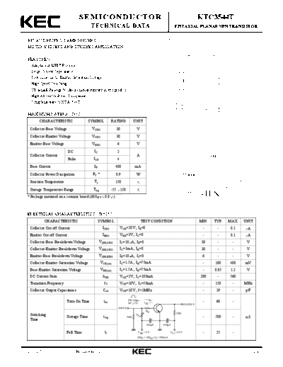
         CHARACTERISTIC                  SYMBOL             RATING              UNIT
                                                                                                                       1. EMITTER
   Collector-Base Voltage                   VCBO                  30             V                                     2. BASE
                                                                                                                       3. COLLECTOR
   Collector-Emitter Voltage                VCEO                  30             V
   Emitter-Base Voltage                     VEBO                   6             V
                             DC              IC                    2
   Collector Current                                                             A                                                          TSM
                             Pulse          ICP                    4
   Base Current                              IB                   400           mA
   Collector Power Dissipation              PC *                  0.9            W                                   Marking
   Junction Temperature                      Tj                   150                                                                                              Lot No.

   Storage Temperature Range                Tstg            -55 150
 * Package mounted on a ceramic board (600            0.8     )
                                                                                                                Type Name
                                                                                                                                            HN

 ELECTRICAL CHARACTERISTICS (Ta=25 )
              CHARACTERISTIC                      SYMBOL                              TEST CONDITION                             MIN.               TYP.     MAX.              UNIT
   Collector Cut-off Current                         ICBO              VCB=20V, IE=0                                                    -               -         0.1                 A
   Emitter Cut-off Current                           IEBO              VEB=3V, IC=0                                                     -               -         0.1                 A
   Collector-Base Breakdown Voltage                V(BR)CBO            IC=10 A, IE=0                                                30                  -          -              V
   Collector-Emitter Breakdown Voltage             V(BR)CEO            IC=1mA, IB=0                                                 30                  -          -              V
   Emitter-Base Breakdown Voltage                  V(BR)EBO            IE=10 A, IC=0                                                    6               -          -              V
   Collector-Emitter Saturation Voltage            VCE(sat)            IC=1.5A, IB=75mA                                                 -           180           400           mV
   Base-Emitter Saturation Voltage                 VBE(sat)            IC=1.5A, IB=75mA                                                 -           0.85          1.2             V
   DC Current Gain                                   hFE               VCE=2V, IC=100mA                                          200                    -         560
   Transition Frequency                               fT               VCE=10V, IC=50mA                                                 -           150            -           MHz
   Collector Output Capacitance                      Cob               VCB=10V, f=1MHz                                                  -            19            -             pF

                                                                           PW=20


◦ Jabse Service Manual Search 2024 ◦ Jabse PravopisonTap.bg ◦ Other service manual resources online : FixyaeServiceinfo