Service Manuals, User Guides, Schematic Diagrams or docs for : . Electronic Components Datasheets Active components Transistors KEC ktc3660u
<< Back | HomeMost service manuals and schematics are PDF files, so You will need Adobre Acrobat Reader to view : Acrobat Download Some of the files are DjVu format. Readers and resources available here : DjVu Resources
For the compressed files, most common are zip and rar. Please, extract files with Your favorite compression software ( WinZip, WinRAR ... ) before viewing. If a document has multiple parts, You should download all, before extracting.
Good luck. Repair on Your own risk. Make sure You know what You are doing.
Image preview - the first page of the document
>> Download ktc3660u documenatation <<
Text preview - extract from the document
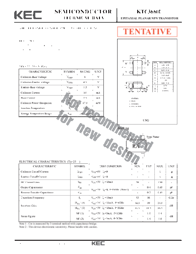
SEMICONDUCTOR KTC3660U
TECHNICAL DATA EPITAXIAL PLANAR NPN TRANSISTOR
VHF/UHF BAND LOW NOISE AMPLIFIER APPLICATIONS.
TENTATIVE
FEATURES
Low Noise Figure, High Gain.
NF=1.4dB (f=2GHz), |S21e|2=13.5dB (f=2GHz).
E
M B M
1 4 D DIM MILLIMETERS
A _
2.00 + 0.20
MAXIMUM RATING (Ta=25 ) _
A
B 1.25 + 0.15
J
C _
0.90 + 0.10
CHARACTERISTIC SYMBOL RATING UNIT 2 3 D 0.3+0.10/-0.05
E _
2.10 + 0.20
Collector-Base Voltage VCBO 8 V H 0.15+0.1/-0.06
J 1.30
Collector-Emitter Voltage VCEO 4.5 V K 0.00 ~ 0.10
C
H 0.70
L
L
Emitter-Base Voltage VEBO 1.5 V M 0.42
N N N 0.10 MIN
K
Collector Current IC 15 mA
Base Current IB 7.5 mA 1. EMITTER
2. BASE
Collector Power Dissipation PC 67.5 mW 3. EMITTER
4. COLLECTOR
Junction Temperature Tj 125
Storage Temperature Range Tstg -55 125
USQ
Marking
4 3
Type Name
RA
1 2
ELECTRICAL CHARACTERISTICS (Ta=25 )
CHARACTERISTIC SYMBOL TEST CONDITION MIN. TYP. MAX. UNIT
Collector Cut-off Current ICBO VCB=8V, IE=0 - - 1 A
Emitter Cut-off Current IEBO VEB=1V, IC=0 - - 1 A
DC Current Gain hFE VCE=3V, IC=10mA 50 - 150 -
Output Capacitance Cob - 0.4 0.65 pF
VCB=3V, IE=0, f=1MHz (Note1)
Reverse Transfer Capacitance Cre - 0.2 0.45 pF
Transition Frequency fT VCE=3V, IC=10mA 13 16 - GHz
|S21e|2 (1) VCE=3V, IC=10mA, f=1GHz 16.5 19 21.5
Insertion Gain dB
|S21e|2 (2) VCE=3V, IC=10mA, f=2GHz 11.5 13.5 16.5
NF (1) VCE=3V, IC=3mA, f=1GHz - 1.0 1.4
Noise Figure dB
NF (2) VCE=3V, IC=3mA, f=2GHz - 1.4 1.8
Note 1 : Cre is measured by 3 terminal method with capacitance bridge.
Note 2 : This device electrostatic sensitivity. Please handle with caution.
2007. 7. 3 Revision No : 0 1/3
KTC3660U
Cob, Cre - VCB f T - IC
REVERSE TRANSFER CAPACITANCE Cre (pF)
TRANSITION FREQUENCY fT (GHz)
1 25
OUTPUT CAPACITANCE Cob (pF)
f=1MHz Ta=25 C
Ta=25 C
20
Cob VCE=3V
0.5
15
0.3 VCE=1V
Cre
10
5
0.1 0
0.1 0.3 0.5 1 3 5 10 1 3 10 30 100
COLLECTOR-BASE VOLTAGE VCB (V) COLLECTOR CURRENT IC (mA)
2 2
S2le - IC S2le - IC
25 25
S2le (dB)
S2le (dB)
f=1GHz f=2GHz
Ta=25 C Ta=25 C
VCE=3V
2
2
20 20
15 VCE=1V 15 VCE=3V
INSERTION CAIN
INSERTION CAIN
10 10 VCE=1V
5 5
0 0
1 3 10 30 100 1 3 10 30 100
COLLECTOR CURRENT IC (mA) COLLECTOR CURRENT IC (mA)
2 2
S2le - f S2le - f
30 30
VCE=1V VCE=3V
S2le (dB)
S2le (dB)
Ta=25 C Ta=25 C
2
2
20 20
INSERTION CAIN
INSERTION CAIN
IC=10mA
IC=10mA
IC=3mA
10 10
IC=3mA
0 0
100 300 1000 3000 10000 100 300 1000 3000 10000
FREQUENCY f (MHz) FREQUENCY f (MHz)
2007. 7. 3 Revision No : 0 2/3
KTC3660U
NF - IC NF - IC
3 3
VCE=1V VCE=3V
NOISE FIGURE NF (dB)
f=1GHz f=1GHz
NOISE FIGURE NF (dB)
Ta=25 C Ta=25 C
2 2
1 1
0 0
1 3 10 30 100 1 3 10 30 100
COLLECTOR CURRENT IC (mA) COLLECTOR CURRENT IC (mA)
NF - IC NF - IC
3 3
VCE=1V VCE=3V
NOISE FIGURE NF (dB)
NOISE FIGURE NF (dB)
f=2GHz f=2GHz
Ta=25 C Ta=25 C
2 2
1 1
0 0
1 3 10 30 100 1 3 10 30 100
COLLECTOR CURRENT IC (mA) COLLECTOR CURRENT IC (mA)
2007. 7. 3 Revision No : 0 3/3
◦ Jabse Service Manual Search 2024 ◦ Jabse Pravopis ◦ onTap.bg ◦ Other service manual resources online : Fixya ◦ eServiceinfo