Service Manuals, User Guides, Schematic Diagrams or docs for : . Electronic Components Datasheets Active components Transistors KEC ktc9018s

<< Back | Home

Most service manuals and schematics are PDF files, so You will need Adobre Acrobat Reader to view : Acrobat Download Some of the files are DjVu format. Readers and resources available here : DjVu Resources
For the compressed files, most common are zip and rar. Please, extract files with Your favorite compression software ( WinZip, WinRAR ... ) before viewing. If a document has multiple parts, You should download all, before extracting.
Good luck. Repair on Your own risk. Make sure You know what You are doing.


Image preview - the first page of the document
ktc9018s


>> Download ktc9018s documenatation <<

Text preview - extract from the document
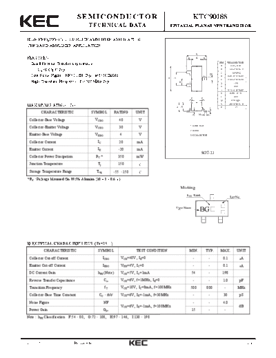
                                   SEMICONDUCTOR                                                                             KTC9018S
                                              TECHNICAL DATA                                             EPITAXIAL PLANAR NPN TRANSISTOR


  HIGH FREQUENCY LOW NOISE AMPLIFIER APPLICATION.
  VHF BAND AMPLIFIER APPLICATION.
                                                                                                                                 E
  FEATURES                                                                                                          L            B           L
                                                                                                                                                        DIM       MILLIMETERS
    Small Reverse Transfer Capacitance                                                                                                                   A                _
                                                                                                                                                                     2.93 + 0.20
      : Cre=0.65pF(Typ.).                                                                                                                                B        1.30+0.20/-0.15
                                                                                                                                                         C           1.30 MAX
    Low Noise Figure : NF=2.2dB(Typ.) at f=100MHz.


                                                                                                                                                  D
                                                                                                                     2                       3           D        0.45+0.15/-0.05


                                                                                                        A

                                                                                                            G
                                                                                                                                                         E        2.40+0.30/-0.20
    High Transition Frequency : fT=800MHz(Typ.).


                                                                                                                H
                                                                                                                     1                                   G              1.90
                                                                                                                                                         H              0.95
                                                                                                                                                         J        0.13+0.10/-0.05
                                                                                                                                                         K          0.00 ~ 0.10
                                                                                                                                                         L              0.55
                                                                                                                         P               P
                                                                                                                                                         M           0.20 MIN
                                                                                                                                                         N        1.00+0.20/-0.10
  MAXIMUM RATING (Ta=25                   )                                                                                                              P                7


                                                                                                                N
                                                                                                            C


                                                                                                                                                  J
              CHARACTERISTIC                   SYMBOL                RATING           UNIT
                                                                                                                                     M


                                                                                                                         K
   Collector-Base Voltage                        VCBO                     40            V
                                                                                                                        1. EMITTER
   Collector-Emitter Voltage                     VCEO                     30            V
                                                                                                                        2. BASE
   Emitter-Base Voltage                          VEBO                      4            V                               3. COLLECTOR

   Collector Current                                  IC                  20           mA
   Emitter Current                                    IE                  -20          mA
                                                                                                                                     SOT-23
   Collector Power Dissipation                       PC *                 350          mW
   Junction Temperature                               Tj                  150
   Storage Temperature Range                         Tstg            -55 150
  * PC : Package Mounted On 99.5% Alumina (10 8                    0.6    )

                                                                                                                Marking
                                                                                                                    h FE Rank                                       Lot No.


                                                                                                            Type Name
                                                                                                                                     BG


  ELECTRICAL CHARACTERISTICS (Ta=25 )
               CHARACTERISTIC                         SYMBOL                           TEST CONDITION                MIN.                        TYP.   MAX.              UNIT
   Collector Cut-off Current                                ICBO              VCB=40V, IE=0                                  -                    -       0.1                 A
   Emitter Cut-off Current                                  IEBO              VEB=4V, IC=0                                   -                    -       0.1                 A
   DC Current Gain                                    hFE (Note)              VCE=5V, IC=1mA                             54                       -       198
   Reverse Transfer Capacitance                             Cre               VCE=6V, f=1MHz, IE=0                           -                    -       1.0               pF
   Transition Frequency                                      fT               VCE=10V, IC=8mA, f=100MHz                  500                     800          -            MHz
   Collector-Base Time Constant                       CC rbb'                 VCE=6V, IE=-1mA, f=30MHz                       -                    -       30                pS
   Noise Figure                                             NF                                                               -                    -       4.0
                                                                              VCE=6V, IE=-1mA, f=100MHz                                                                     dB
   Power Gain                                               Gpe                                                          15                       -           -
  Note : hFE Classification    F:54 80,       G:72     108,        H:97       146,   I:130 198


2003. 3. 25                      Revision No : 1                                                                                                                                    1/3
                                                                                                                                      KTC9018S


                                                                             STATIC CHARACTERISTICS                                                                                                                                                          h FE - I C
                                                                                                                                                                                                           300
                                       20                                                                500                                                                                                                          COMMON EMITTER
                 COLLECTOR CURRENT


                                                                                                         450
                                                                                                          400                                                                                                                         VCE =6V


                                                                                                                                                                            DC CURRENT GAIN h FE
                                       16                                                                 350
                                                                                                           300                                                                                                                        Ta=25 C
                       I C (mA)


                                                                                                           250                                                                                             100
                                       12
                                                                            VCE =6V                         200
                                             8                                                                150
                                                                                                                 100                                                                                              50
                                             4                                                                   I B =50


◦ Jabse Service Manual Search 2024 ◦ Jabse PravopisonTap.bg ◦ Other service manual resources online : FixyaeServiceinfo