Service Manuals, User Guides, Schematic Diagrams or docs for : . Electronic Components Datasheets Active components Transistors KEC ktd1824

<< Back | Home

Most service manuals and schematics are PDF files, so You will need Adobre Acrobat Reader to view : Acrobat Download Some of the files are DjVu format. Readers and resources available here : DjVu Resources
For the compressed files, most common are zip and rar. Please, extract files with Your favorite compression software ( WinZip, WinRAR ... ) before viewing. If a document has multiple parts, You should download all, before extracting.
Good luck. Repair on Your own risk. Make sure You know what You are doing.


Image preview - the first page of the document
ktd1824


>> Download ktd1824 documenatation <<

Text preview - extract from the document
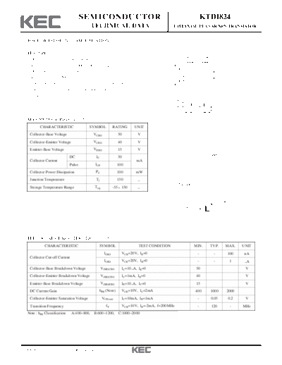
                                      SEMICONDUCTOR                                                                               KTD1824
                                              TECHNICAL DATA                                          EPITAXIAL PLANAR NPN TRANSISTOR


  FOR LOW-FREQUENCY AMPLIFICATION.

  FEATURES
                                                                                                                            E
    High foward current transfer ratio hFE.                                                                        M        B      M
    Low collector to emitter saturation voltage VCE(sat).                                                                                           DIM    MILLIMETERS
                                                                                                                                                     A            _
                                                                                                                                                             2.00 + 0.20
                                                                                                                                                D
    High emitter to base voltage VEBO.                                                                                2                             B             _
                                                                                                                                                             1.25 + 0.15
                                                                                                                                                                  _


                                                                                                      A
                                                                                                                                                             0.90 + 0.10


                                                                                                          J
                                                                                                                                                    C
    Low noise voltage NV.                                                                                             1            3


                                                                                                              G
                                                                                                                                                    D      0.3+0.10/-0.05
    USM type package, allowing downsizing of the equipment and                                                                                      E             _
                                                                                                                                                             2.10 + 0.20
                                                                                                                                                    G               0.65
    automatic insertion through the tape packing and the magazine                                                                                   H          0.15+0.1/-0.06
                                                                                                                                                    J               1.30
    packing.
                                                                                                                                                    K            0.00-0.10
                                                                                                                                                    L               0.70


                                                                                                          C
                                                                                                                                            H                         _


                                                                                                              L
                                                                                                                                                    M            0.42 + 0.10
                                                                                                                                                    N            0.10 MIN
                                                                                                                  N                    N
                                                                                                                          K


  MAXIMUM RATINGS (Ta=25                  )
                                                                                                                  1. EMITTER
          CHARACTERISTIC                   SYMBOL             RATING           UNIT
                                                                                                                  2. BASE
   Collector-Base Voltage                     VCBO                    50             V                            3. COLLECTOR

   Collector-Emitter Voltage                  VCEO                    40             V
   Emitter-Base Voltage                       VEBO                    15             V
                              DC               IC                     50                                                               USM
   Collector Current                                                            mA
                              Pulse            ICP                  100
   Collector Power Dissipation                 PC                   100        mW
   Junction Temperature                        Tj                   150         


◦ Jabse Service Manual Search 2024 ◦ Jabse PravopisonTap.bg ◦ Other service manual resources online : FixyaeServiceinfo