Service Manuals, User Guides, Schematic Diagrams or docs for : . Electronic Components Datasheets Active components Transistors KEC ktk920bt

<< Back | Home

Most service manuals and schematics are PDF files, so You will need Adobre Acrobat Reader to view : Acrobat Download Some of the files are DjVu format. Readers and resources available here : DjVu Resources
For the compressed files, most common are zip and rar. Please, extract files with Your favorite compression software ( WinZip, WinRAR ... ) before viewing. If a document has multiple parts, You should download all, before extracting.
Good luck. Repair on Your own risk. Make sure You know what You are doing.


Image preview - the first page of the document
ktk920bt


>> Download ktk920bt documenatation <<

Text preview - extract from the document
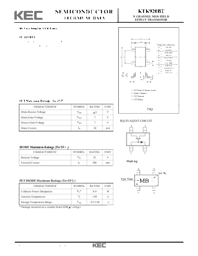
                                  SEMICONDUCTOR                                                          KTK920BT
                                                                                                     N CHANNEL MOS FIELD
                                          TECHNICAL DATA                                              EFFECT TRANSISTOR


  RF Switching for VCR Tuner

  FEATURES                                                                                                   E
    Low loss at on state(Typ 1dB@1GHz)                                                                       B
                                                                                                                                         DIM MILLIMETERS
    With built-in bias diode                                                                                                              A         _
                                                                                                                                                2.9 + 0.2
                                                                                                     1               4
                                                                                                                                          B    1.6+0.2/-0.1
                                                                                                                                          C          _
                                                                                                                                                0.70 + 0.05
                                                                                                                                          D          _
                                                                                                                                                 0.4 + 0.1


                                                                                     F
                                                                                 A
                                                                                                                                          E    2.8+0.2/-0.3
                                                                                                                                          F          _
                                                                                                                                                 1.9 + 0.2
                                                                                                     2               3
                                                                                                                                          G          _
                                                                                                                                                0.16 + 0.05


                                                                                                                                 D
                                                                                                                                          H      0.00-0.10
                                                                                                                                          I    0.25+0.3/-0.15
                                                                                                                                          J           _
                                                                                                                                                 0.60 + 0.1
                                                                                                                                          K           _
                                                                                                                                                 0.55 + 0.1


                                                                                         K
                                                                                 C
                                                                                                 I           H           I   G


                                                                                                 1. FET Gate & Diode Anode
                                                                                                 2. Diode Cathode
                                                                                                 3. FET Source
                                                                                                 4. FET Drain
  FET Maximum Ratings (Ta=25             )
              CHARACTERISTIC                       SYMBOL       RATING    UNIT
                                                                                                                     TSQ
   Drain-Source-Voltage                                VDS          3      V
   Drain-Gate-Voltage                                  VDG        7        V
                                                                                 EQUIVALENT CIRCUIT
   Source-Gate-Voltage                                 VSG        7        V
                                                                                             4                   3
   Drain Current                                         ID       10      mA


  DIODE Maximum Ratings (Ta=25               )
              CHARACTERISTIC                       SYMBOL       RATING    UNIT               1                   2
   Reverse Voltage                                       VR       35       V
   Forword Current                                       IF      100      mA             Marking

                                                                                                         4                           3
                                                                                                                                          Lot No.

                                                                                 Type Name
  FET DIODE Maximum Ratings (Ta=25                 )                                                         MB
              CHARACTERISTIC                       SYMBOL       RATING    UNIT
   Collector Power Dissipation                           PC*      0.9      W                             1                           2
   Junction Temperature                                  Tj      150
   Storage Temperature Range                             Tstg   -55~150
  * Package mounted on a ceramic board (600        0.8     )


2007. 5. 29                      Revision No : 1                                                                                                                1/3
                                                                            KTK920BT

 FET ELECTRICAL CHARACTERISTICS (Ta=25                                            )
               CHARACTERISTIC                            SYMBOL                           TEST CONDITIONS                 MIN   TYP    MAX    UNIT
   Gate-Source Breakdown Voltage                           V(BR)GSS       VDS=0, IGS=-0.1mA                                7     -      -      V
   Gate-Source Pinch-off Voltage                           VGS(OFF)       VDS=1V, ID=20 A                                  -     -3     -4     V
   Drain-Source Leakage Current                              IDSX         VDS=2V, VGS=-5V                                  -     -     10      A
   Gate Cut-off Current                                      IGSS         VDS=0, VGS=-5V                                   -     -     -100    nA
   Drain-Source On-State Resistance                        RDS(ON)        VGS=0, ID=1mA                                    -    12     20
                                                                          VSC=VDC=0, RS=RL=50     , IF=0, f   1GHz         -     -      2      dB
   Loss(On-State)                                          S21(ON) 2      VSC=VDC=0, RS=RL=50     , IF=0, f=1GHz           -    1.3     -      dB
                                                                          VSC=VDC=0, RS=RL=75     , IF=0, f   1GHz         -     -      3      dB
                                                                          VSC=VDC=5V, RS=RL=50      , IF=1mA, f    1GHz   30     -      -      dB
   Isolation (Off-State)                                   S21(OFF) 2     VSC=VDC=5V, RS=RL=50      , IF=1mA, f= 1GHz      -    38      -      dB
                                                                          VSC=VDC=5V, RS=RL=75      , IF=1mA, f    1GHz   30     -      -      dB
                                                                          VSC=VDC=5V, IF=1mA, f=1MHz                       -     1      -      pF
   Input Capacitance Note1                                    Cic
                                                                          VSC=VDC=0, IF=0, f=1MHz                          -    0.65    -      pF
                                                                          VSC=VDC=5V, IF=1mA, f=1MHz                       -     1      -      pF
   Output Capacitance Note1                                   Coc
                                                                          VSC=VDC=0, IF=0, f=1MHz                          -    0.65    -      pF
 Note : 1 Cic is the series connection of Csg and Cgc;
          Coc is the series connection of Cdg and Cgc;


 DIODE ELECTRICAL CHARACTERISTICS (Ta=25                                              )
               CHARACTERISTIC                            SYMBOL                           TEST CONDITIONS                 MIN   TYP    MAX    UNIT
    Forward Voltage                                           VF           IF=2mA                                          -     -     0.85    V
    Reverse Current                                             IR         VR=15V                                          -     -     0.1
    Reverse Voltage                                           VR           IR=1                                           35     -      -      V
    Total Capacitance                                         CT           VR=6V, f=1MHz                                   -    0.7    1.2     pF
    Series Resistance                                           rS         IF=2mA, f=100MHz                                -    0.5    0.9


  Fig. S21(on) 2    S21(off)   2
                                   Test Circuit

                        1nF            V


                       100k
                                                    On-State : V=0V
                                                    Off-State : V=5V
                           47k

           50                                                           50
           Output                                                       Input
                         1nF                                 1nF


                         4.7k
                       100k


                         1nF
                                       V


2007. 5. 29                                   Revision No : 1                                                                                       2/3
                                                                           KTK920BT


                                                     2                                                                                             2
                                           S21(ON)       - f                                                                            S21(OFF)       - f

                               0                                                                                 2 0
                                                                                      S21(OFF)                          VSC=VDC=5V, RS=RL=50 , IF = 1mA
                           2
      S21(ON)                                                                           (dB)                            Measured in test circuit (fig.)

       (dB)


                                                                                         ISOLATION (OFF-STATE)
                               -1
                                                                                                                 -20
         LOSS (ON-STATE)


                               -2

                                                                                                                 -40
                               -3
                                                  VSC=VDC=0V, RS=RL=50
                                                  IF = 0mA
                                                  Measured in test circuit (fig.)
                               -4                                                                                -60
                                    0    400               800                 1200                                 0                400                800   1200


                                        FREQUENCY f (MHz)                                                                         FREQUENCY f (MHz)


2007. 5. 29                                Revision No : 1                                                                                                           3/3


◦ Jabse Service Manual Search 2024 ◦ Jabse PravopisonTap.bg ◦ Other service manual resources online : FixyaeServiceinfo