Service Manuals, User Guides, Schematic Diagrams or docs for : . Electronic Components Datasheets Active components Transistors KEC ktx211e

<< Back | Home

Most service manuals and schematics are PDF files, so You will need Adobre Acrobat Reader to view : Acrobat Download Some of the files are DjVu format. Readers and resources available here : DjVu Resources
For the compressed files, most common are zip and rar. Please, extract files with Your favorite compression software ( WinZip, WinRAR ... ) before viewing. If a document has multiple parts, You should download all, before extracting.
Good luck. Repair on Your own risk. Make sure You know what You are doing.


Image preview - the first page of the document
ktx211e


>> Download ktx211e documenatation <<

Text preview - extract from the document
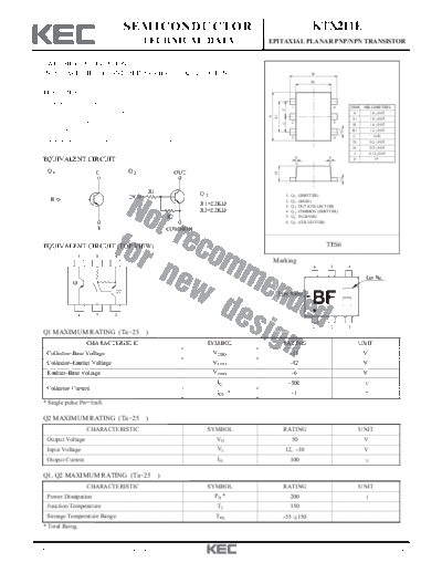
                                     SEMICONDUCTOR                                                                 KTX211E
                                             TECHNICAL DATA                         EPITAXIAL PLANAR PNP/NPN TRANSISTOR


  SWITCHING APPLICATION.
  INTERFACE CIRCUIT AND DRIVER CIRCUIT APPLICATION.                                                                B

                                                                                                                   B1

  FEATURES
    Including two devices in TES6.
                                                                                                      1                        6           DIM   MILLIMETERS


                                                                                             C
    (Thin Extreme Super mini type with 6 leads.)                                                                                            A           _
                                                                                                                                                    1.6 + 0.05


                                                                                        A1
                                                                                    A
                                                                                                                                            A1          _
                                                                                                                                                    1.0 + 0.05
    With Built-in bias resistors.                                                                     2                        5


                                                                                             C
                                                                                                                                            B           _
                                                                                                                                                    1.6 + 0.05
    Simplify circuit design.                                                                                                                B1          _
                                                                                                                                                    1.2 + 0.05


                                                                                                                                   D
                                                                                                      3                        4            C          0.50
    Reduce a quantity of parts and manufacturing process.                                                                                   D           _
                                                                                                                                                    0.2 + 0.05
                                                                                                                                            H           _
                                                                                                                                                    0.5 + 0.05
                                                                                                                                             J           _
                                                                                                                                                   0.12 + 0.05
                                                                                                          P
  EQUIVALENT CIRCUIT                                                                                                      P                 P           5


   Q1                   C              Q2                       OUT


                                                                                        H


                                                                                                                                   J
                                                  R1                  Q2
                                        IN                                                       1.   Q1      (EMITTER)
    B                                                                                            2.   Q1      (BASE)
                                                                      R1=2.2K                    3.   Q2      OUT (COLLECTOR)
                                                                      R2=2.2K                    4.   Q2      COMMON (EMITTER)
                                                           R2                                    5.   Q2      IN (BASE)
                                                                                                 6.   Q1      (COLLECTOR)
                        E                                  COMMON

  EQUIVALENT CIRCUIT (TOP VIEW)                                                                                          TES6
                6       5       4
                                                                                        Marking
                                                                                                                    6      5           4

                                                                                                                                                  Lot No.
              Q1


                                                                                                                   BF
                                Q2                                                       Type Name


                1       2       3

                                                                                                                   1       2           3
  Q1 MAXIMUM RATING (Ta=25                    )
                    CHARACTERISTIC                                     SYMBOL                RATING                                          UNIT
   Collector-Base Voltage                                                  VCBO                       -15                                        V
   Collector-Emitter Voltage                                               VCEO                       -12                                        V
   Emitter-Base Voltage                                                    VEBO                       -6                                         V
                                                                            IC                    -500
   Collector Current
                                                                            ICP *                     -1
  * Single pulse Pw=1mS.

  Q2 MAXIMUM RATING (Ta=25                    )
                    CHARACTERISTIC                                     SYMBOL                RATING                                          UNIT
   Output Voltage                                                          VO                         50                                         V
   Input Voltage                                                            VI                   12, -10                                         V
   Output Current                                                           IO                        100

  Q1, Q2 MAXIMUM RATING (Ta=25                         )
                    CHARACTERISTIC                                     SYMBOL                RATING                                          UNIT
   Power Dissipation                                                       PD *                       200
   Junction Temperature                                                     Tj                        150
   Storage Temperature Range                                               Tstg              -55 150
  * Total Raing.


2008. 9. 23                         Revision No : 1                                                                                                              1/4
                                                                   KTX211E

 Q1 ELECTRICAL CHARACTERISTICS (Ta=25                          )
              CHARACTERISTIC                   SYMBOL                         TEST CONDITION       MIN.      TYP.    MAX.      UNIT
   Collector Cut-off Current                         ICBO          VCB=-15V, IE=0                       -        -    -100      nA
   Collector-Base Breakdown Voltage             V(BR)CBO           IE=-10 A                         -15          -         -     V
   Collector-Emitter Breakdown Voltage          V(BR)CEO           IC=-1mA                          -12          -         -     V
   Emitter-Base Breakdown Voltage               V(BR)EBO           IE=-10 A                            -6        -         -     V
   DC Current Gain                                    hFE          VCE=-2V, IC=-10mA                270          -    680        -
   Collector-Emitter Saturation Voltage             VCE(sat)       IC=-200mA, IB=-10mA                  -    -100     -250      mV
   Transition Frequency                               fT           VCE=-2V, IC=-10mA, fT=100MHz         -    260           -   MHz
   Collector Output Capacitance                       Cob          VCB=-10V, IE=0, f=1MHz               -    6.5           -    pF


 Q2 ELECTRICAL CHARACTERISTICS (Ta=25                          )
              CHARACTERISTIC                  SYMBOL                        TEST CONDITION        MIN.      TYP.     MAX.      UNIT.
   Output Cut-off Current                       IO(OFF)            VO=50V, VI=0                    -         -       500
   DC Current Gain                                   GI            VO=5V, IO=20                    20        -         -
   Output Voltage                               VO(ON)             IO=10   , II=0.5                -        0.1       0.3       V
   Input Voltage (ON)                           VI(ON)             VO=0.3V, IO=20                  -        1.83      3         V
   Input Voltage (OFF)                          VI(OFF)            VO=5V, IO=0.1                  0.5       1.15       -        V
   Transition Frequency                             fT *           VO=10V, IO=5                    -        250        -
   Input Current                                     II            VI=5V                           -         -        3.8
 Note : * Characteristic of Transistor Only.


2008. 9. 23                       Revision No : 1                                                                                      2/4
                                KTX211E


2008. 9. 23   Revision No : 1             3/4
                                KTX211E


2008. 9. 23   Revision No : 1             4/4


◦ Jabse Service Manual Search 2024 ◦ Jabse PravopisonTap.bg ◦ Other service manual resources online : FixyaeServiceinfo