Service Manuals, User Guides, Schematic Diagrams or docs for : . Electronic Components Datasheets Active components Transistors KEC ktx312t

<< Back | Home

Most service manuals and schematics are PDF files, so You will need Adobre Acrobat Reader to view : Acrobat Download Some of the files are DjVu format. Readers and resources available here : DjVu Resources
For the compressed files, most common are zip and rar. Please, extract files with Your favorite compression software ( WinZip, WinRAR ... ) before viewing. If a document has multiple parts, You should download all, before extracting.
Good luck. Repair on Your own risk. Make sure You know what You are doing.


Image preview - the first page of the document
ktx312t


>> Download ktx312t documenatation <<

Text preview - extract from the document
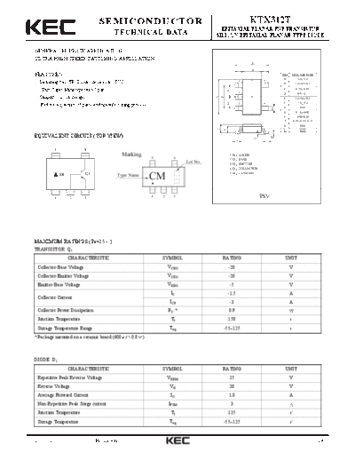
                                  SEMICONDUCTOR                                                                KTX312T
                                                                                        EPITAXIAL PLANAR PNP TRANSISTOR
                                            TECHNICAL DATA                            SILICON EPITAXIAL PLANAR TYPE DIODE

  GENERAL PURPOSE APPLICATION.
  ULTRA HIGH SPEED SWITCHING APPLICATION.
                                                                                                                E

                                                                                                                B
  FEATURES                                                                                                                           DIM   MILLIMETERS
                                                                                                                                      A           _
                                                                                                                                              2.9 + 0.2
                                                                                                          1              5
    Including two(TR, Diode) devices in TSV.                                                                                          B     1.6+0.2/-0.1
                                                                                                                                                  _
    (Thin Super Mini type with 5 pin)                                                                                                 C      0.70 + 0.05


                                                                                              G
                                                                                                          2                                       _
                                                                                                                                     D        0.4 + 0.1
    Simplify circuit design.


                                                                                          F
                                                                                      A
                                                                                                                                     E         2.8+0.2/-0.3
                                                                                                          3              4           F               _
                                                                                                                                                 1.9 + 0.2
     Reduce a quantity of parts and manufacturing process.


                                                                                              G
                                                                                                                                     G             0.95


                                                                                                                                 D
                                                                                                                                     H               _
                                                                                                                                                0.16 + 0.05
                                                                                                                                     I        0.00-0.10
                                                                                                                                     J     0.25+0.25/-0.15
                                                                                                                                     K           0.60


                                                                                      C
                                                                                                                                     L           0.55


                                                                                          L
 EQUIVALENT CIRCUIT (TOP VIEW)                                                                                      I            H
                                                                                                      J                      J


              5             4
                                             Marking         5         4
                                                                                              1. D 1      ANODE
                                                                                              2. Q 1      BASE
                                                                            Lot No.           3. Q 1      EMITTER
                                                                                              4. Q 1      COLLECTOR
                  D1        Q1              Type Name
                                                             CM                               5. D 1      CATHODE


              1        2    3
                                                             1   2     3                                                TSV


 MAXIMUM RATINGS (Ta=25                 )
 TRANSISTOR Q1
                       CHARACTERISTIC                            SYMBOL                   RATING                                      UNIT
   Collector-Base Voltage                                            VCBO                     -20                                          V
   Collector-Emitter Voltage                                         VCEO                     -20                                          V
   Emitter-Base Voltage                                              VEBO                     -5                                           V
                                                                      IC                      -1.5                                         A
   Collector Current
                                                                     ICP                      -3                                           A
   Collector Power Dissipation                                       PC *                     0.9
   Junction Temperature                                               Tj                      150
   Storage Temperature Range                                         Tstg                 -55~125
 * Package mounted on a ceramic board (600         0.8   )


 DIODE D1
                       CHARACTERISTIC                            SYMBOL                   RATING                                      UNIT
   Repetitive Peak Reverse Voltage                                   VRRM                     25                                           V
   Reverse Voltage                                                   VR                       20                                           V
   Average Forward Current                                            IO                      1.0                                          A
   Non-Repetitive Peak Surge current                                 IFSM                         3
   Junction Temperature                                               Tj                      125
   Storage Temperature                                               Tstg                 -55~125


2003. 3. 11                      Revision No : 1                                                                                                              1/4
                                                                  KTX312T


 ELECTRICAL CHARACTERISTICS (Ta=25 )
 TRANSISTOR Q1

              CHARACTERISTIC                SYMBOL                              TEST CONDITION                             MIN.      TYP.     MAX.    UNIT
   Collector Cut-off Current                   ICBO            VCB=-12V, IE=0                                                  -          -    -0.1     A
   Emitter Cut-off Current                     IEBO            VEB=-4V, IC=0                                                   -          -    -0.1     A
   Collector-Base Breakdown Voltage          V(BR)CBO          IC=-10 A, IE=0                                                 -20         -     -       V
   Collector-Emitter Breakdown Voltage       V(BR)CEO          IC=-1mA, IB=0                                                  -20         -     -       V
   Emitter-Base Breakdown Voltage            V(BR)EBO          IE=-10 A, IC=0                                                 -5          -     -       V
   Collector-Emitter Saturation Voltage       VCE(sat)         IC=-750mA, IB=-15mA                                             -     -120      -180    mV
   Base-Emitter Saturation Voltage            VBE(sat)         IC=-750mA, IB=-15mA                                             -     -0.85     -1.2     V
   DC Current Gain                              hFE            VCE=-2V, IC=-100mA                                             200         -    560
   Transition Frequency                         fT             VCE=-2V, IC=-300mA                                              -      210       -     MHz
   Collector Output Capacitance                 Cob            VCB=-10V, f=1MHz                                                -         30     -      pF

                                                                      PW=20


◦ Jabse Service Manual Search 2024 ◦ Jabse PravopisonTap.bg ◦ Other service manual resources online : FixyaeServiceinfo