Service Manuals, User Guides, Schematic Diagrams or docs for : . Electronic Components Datasheets Active components Transistors KEC ktx511t

<< Back | Home

Most service manuals and schematics are PDF files, so You will need Adobre Acrobat Reader to view : Acrobat Download Some of the files are DjVu format. Readers and resources available here : DjVu Resources
For the compressed files, most common are zip and rar. Please, extract files with Your favorite compression software ( WinZip, WinRAR ... ) before viewing. If a document has multiple parts, You should download all, before extracting.
Good luck. Repair on Your own risk. Make sure You know what You are doing.


Image preview - the first page of the document
ktx511t


>> Download ktx511t documenatation <<

Text preview - extract from the document
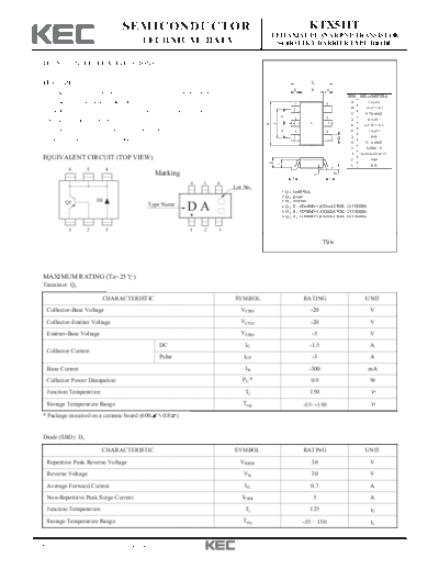
                                    SEMICONDUCTOR                                                              KTX511T
                                                                                          EPITAXIAL PLANAR PNP TRANSISTOR
                                              TECHNICAL DATA                               SCHOTTKY BARRIER TYPE DIODE


  DC/DC CONVERTER APPLICATIONS.

  FEATURES                                                                                                      E

                                                                                                       K        B        K
    Composite type with a PNP transistor and a Schottky barrier diode
                                                                                                                                         DIM   MILLIMETERS
    contained in one package facilitating high-density mounting.                                          1              6                A           _
                                                                                                                                                  2.9 + 0.2
                                                                                                                                          B     1.6+0.2/-0.1
    The KTX511T consists of two chips which are equivalent to the                                                                         C           _
                                                                                                                                                 0.70 + 0.05


                                                                                                  G
                                                                                                          2              5                            _
                                                                                                                                                  0.4 + 0.1
    KTA1532T and the KDR701S, respectively.                                                                                               D


                                                                                          F
                                                                                      A
                                                                                                                                          E     2.8+0.2/-0.3
    Ultrasmall-sized package permiting applied sets to be made small                                                                                  _


                                                                                                  G
                                                                                                          3              4                F       1.9 + 0.2
                                                                                                                                          G         0.95


                                                                                                                                     D
    and slim (mounting height 0.7    ).                                                                                                   H           _
                                                                                                                                                 0.16 + 0.05
                                                                                                                                          I      0.00-0.10
                                                                                                                                          J    0.25+0.25/-0.15
  EQUIVALENT CIRCUIT (TOP VIEW)                                                                                                           K         0.60


                                                                                      C

                                                                                              L
                                                                                                                                          L         0.55
               6   5        4
                                                Marking                                                             I
                                                                                                                             J
                                                                                                                                 H
                                                                                                      J
                                                               6   5    4
                                                                            Lot No.
                                                                                                  1. Q 1 EMITTER
                                                                                                  2. Q 1 BASE
              Q1       D1                                                                         3. D 1 ANODE
                                              Type Name
                                                               DA                                 4. Q 1, D 1 COMMON (COLLECTOR, CATHODE)
                                                                                                  5. Q 1, D 1 COMMON (COLLECTOR, CATHODE)
                                                                                                  6. Q 1, D 1 COMMON (COLLECTOR, CATHODE)


               1   2        3                                  1   2    3

                                                                                                                        TS6


  MAXIMUM RATING (Ta=25                   )
  Transistor Q1

                          CHARACTERISTIC                                    SYMBOL                            RATING                             UNIT
   Collector-Base Voltage                                                     VCBO                              -20                                 V
   Collector-Emitter Voltage                                                   VCEO                             -20                                 V
   Emitter-Base Voltage                                                        VEBO                             -5                                  V
                                                   DC                           IC                              -1.5                                A
   Collector Current
                                                   Pulse                        ICP                             -3                                  A
   Base Current                                                                 IB                             -300                                mA
   Collector Power Dissipation                                                 PC *                             0.9                                 W
   Junction Temperature                                                         Tj                              150
   Storage Temperature Range                                                   Tstg                           -55 150
  * Package mounted on a ceramic board (600         0.8    )


  Diode (SBD) D1

                          CHARACTERISTIC                                    SYMBOL                            RATING                             UNIT
   Repetitive Peak Reverse Voltage                                            VRRM                              30                                  V
   Reverse Voltage                                                              VR                              30                                  V
   Average Forward Current                                                      IO                              0.7                                 A
   Non-Repetitive Peak Surge Current                                           IFSM                              5                                  A
   Junction Temperature                                                         Tj                              125
   Storage Temperature Range                                                   Tstg                           -55 150


2002. 1. 24                      Revision No : 1                                                                                                                 1/5
                                                           KTX511T

 ELECTRICAL CHARACTERISTICS (Ta=25 )
 Transistor Q1

              CHARACTERISTIC               SYMBOL                  TEST CONDITION   MIN.   TYP.    MAX.   UNIT
   Collector Cut-off Current                  ICBO     VCB=-12V, IE=0                -       -     -0.1    A
   Emitter Cut-off Current                    IEBO     VEB=-4V, IC=0                 -       -     -0.1    A
   Collector-Base Breakdown Voltage         V(BR)CBO   IC=-10 A, IE=0                20      -      -      V
   Collector-Emitter Breakdown Voltage      V(BR)CEO   IC=-1mA, IB=0                 20      -      -      V
   Emitter-Base Breakdown Voltage           V(BR)EBO   IE=-10 A, IC=0                -5      -      -      V
                                                       IC=-750mA, IB=-15mA           -     -120    -180   mV
   Collector-Emitter Saturation Voltage     VCE(sat)
                                                       IC=-1.5A, IB=-30mA            -     -210    -320   mV
   Base-Emitter Saturation Voltage          VBE(sat)   IC=-750mA, IB=-15mA           -     -0.85   -1.2    V
   DC Current Gain                            hFE      VCE=-2V, IC=-100mA           200      -     560
   Transition Frequency                        fT      VCE=-2V, IC=-300mA            -     210      -     MHz
   Collector Output Capacitance               Cob      VCB=-10V, f=1MHz              -      30      -      pF


                          Turn-On Time         ton                                   -      50      -


   Swiitching                                  tstg
                          Storage Time                                               -      90      -      nS
   Time


                          Fall Time             tf                                   -      15      -


 Diode (SBD) D1

              CHARACTERISTIC                SYMBOL                 TEST CONDITION   MIN.   TYP.    MAX.   UNIT
   Reverse Voltage                              VR      IR=1mA                       30      -      -      V
   Forward Voltage                              VF      IF=0.7A                      -       -     0.55    V
   Reverse Current                               IR     VR=30V                                      80     A
   Total Capacitance                            CT      VR=0V, f=1MHz                -     190      -      pF
   Reverse Recover Time                          trr    IF=IR=100mA                  -     7.5      -      ns


2002. 1. 24                       Revision No : 1                                                                2/5
                                KTX511T


2002. 1. 24   Revision No : 1             3/5
                                KTX511T


2002. 1. 24   Revision No : 1             4/5
                                KTX511T


2002. 1. 24   Revision No : 1             5/5


◦ Jabse Service Manual Search 2024 ◦ Jabse PravopisonTap.bg ◦ Other service manual resources online : FixyaeServiceinfo