Service Manuals, User Guides, Schematic Diagrams or docs for : . Electronic Components Datasheets Active components Transistors KEC kf5n50pz
<< Back | HomeMost service manuals and schematics are PDF files, so You will need Adobre Acrobat Reader to view : Acrobat Download Some of the files are DjVu format. Readers and resources available here : DjVu Resources
For the compressed files, most common are zip and rar. Please, extract files with Your favorite compression software ( WinZip, WinRAR ... ) before viewing. If a document has multiple parts, You should download all, before extracting.
Good luck. Repair on Your own risk. Make sure You know what You are doing.
Image preview - the first page of the document
>> Download kf5n50pz documenatation <<
Text preview - extract from the document
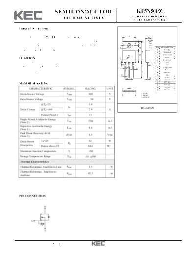
SEMICONDUCTOR KF5N50PZ
N CHANNEL MOS FIELD
TECHNICAL DATA EFFECT TRANSISTOR
General Description
A
This planar stripe MOSFET has better characteristics, such as fast O
C
switching time, low on resistance, low gate charge and excellent
F
avalanche characteristics. It is mainly suitable for electronic ballast and
E G DIM MILLIMETERS
switching mode power supplies. A _
9.9 + 0.2
B B 15.95 MAX
Q C 1.3+0.1/-0.05
D _
0.8 + 0.1
FEATURES I
E _
3.6 + 0.2
VDSS= 500V, ID= 5.0A K
F _
2.8 + 0.1
P G 3.7
Drain-Source ON Resistance : RDS(ON)=1.4 @VGS = 10V M H 0.5+0.1/-0.05
L
I 1.5
Qg(typ) = 12nC J J _
13.08 + 0.3
D K 1.46
L _
1.4 + 0.1
N N H
M _
1.27+ 0.1
N _
2.54 + 0.2
MAXIMUM RATING (Tc=25 ) O _
4.5 + 0.2
P _
2.4 + 0.2
CHARACTERISTIC SYMBOL RATING UNIT Q _
9.2 + 0.2
1 2 3 1. GATE
Drain-Source Voltage VDSS 500 V 2. DRAIN
3. SOURCE
Gate-Source Voltage VGSS 30 V
@TC=25 5.0
ID TO-220AB
Drain Current @TC=100 2.9 A
Pulsed (Note1) IDP 13
Single Pulsed Avalanche Energy EAS 270 mJ
(Note 2)
Repetitive Avalanche Energy EAR 8.6 mJ
(Note 1)
Peak Diode Recovery dv/dt
dv/dt 4.5 V/ns
(Note 3)
Drain Power Tc=25 83 W
PD
Dissipation Derate above 25 0.66 W/
Maximum Junction Temperature Tj 150
Storage Temperature Range Tstg -55 150
Thermal Characteristics
Thermal Resistance, Junction-to-Case RthJC 1.5 /W
Thermal Resistance, Junction-to-
RthJA 62.5 /W
Ambient
PIN CONNECTION
D
G
S
2011. 2. 7 Revision No : 0 1/6
KF5N50PZ
ELECTRICAL CHARACTERISTICS (Tc=25 )
CHARACTERISTIC SYMBOL TEST CONDITION MIN. TYP. MAX. UNIT
Static
Drain-Source Breakdown Voltage BVDSS ID=250 , VGS=0V 500 - - V
Breakdown Voltage Temperature Coefficient BVDSS/ Tj ID=250 , Referenced to 25 - 0.55 - V/
Drain Cut-off Current IDSS VDS=500V, VGS=0V, - - 10
Gate Threshold Voltage Vth VDS=VGS, ID=250 2.5 - 4.5 V
Gate Leakage Current IGSS VGS= 25V, VDS=0V - - 10
Drain-Source ON Resistance RDS(ON) VGS=10V, ID=2.5A - 1.15 1.4
Dynamic
Total Gate Charge Qg - 12 -
VDS=400V, ID=5A
Gate-Source Charge Qgs - 2.4 - nC
VGS=10V (Note4,5)
Gate-Drain Charge Qgd - 5.4 -
Turn-on Delay time td(on) - 22.5 -
VDD=250V
Turn-on Rise time tr - 29 -
RL=50 ns
Turn-off Delay time td(off) - 58 -
RG=25 (Note4,5)
Turn-off Fall time tf - 18 -
Input Capacitance Ciss - 430 -
Output Capacitance Coss VDS=25V, VGS=0V, f=1.0MHz - 71 - pF
Reverse Transfer Capacitance Crss - 7.5 -
Source-Drain Diode Ratings
Continuous Source Current IS - - 5
VGS
◦ Jabse Service Manual Search 2024 ◦ Jabse Pravopis ◦ onTap.bg ◦ Other service manual resources online : Fixya ◦ eServiceinfo