Service Manuals, User Guides, Schematic Diagrams or docs for : . Electronic Components Datasheets Active components Transistors KEC kf60n06p

<< Back | Home

Most service manuals and schematics are PDF files, so You will need Adobre Acrobat Reader to view : Acrobat Download Some of the files are DjVu format. Readers and resources available here : DjVu Resources
For the compressed files, most common are zip and rar. Please, extract files with Your favorite compression software ( WinZip, WinRAR ... ) before viewing. If a document has multiple parts, You should download all, before extracting.
Good luck. Repair on Your own risk. Make sure You know what You are doing.


Image preview - the first page of the document
kf60n06p


>> Download kf60n06p documenatation <<

Text preview - extract from the document
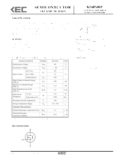
                                   SEMICONDUCTOR                                                                       KF60N06P
                                                                                                               N CHANNEL MOS FIELD
                                          TECHNICAL DATA                                                        EFFECT TRANSISTOR

  General Description

    This planar stripe MOSFET has better characteristics, such as fast                                 A
                                                                                                                                  O
  switching time, low on resistance, low gate charge and excellent                                                                     C
                                                                                                                       F
  avalanche characteristics. It is mainly suitable for active power factor
                                                                                       E                               G                   DIM MILLIMETERS
  correction , electronic lamp ballasts based on half bridge topology,                                                                      A        _
                                                                                                                                                 9.9 + 0.2
                                                                                                                           B
  DC/DC Converters and switching mode power supplies.                                                                                      B     15.95 MAX
                                                                                                                       Q                   C    1.3+0.1/-0.05
                                                                                       I                                                   D           _
                                                                                                                                                   0.8 + 0.1
  FEATURES                                                                                                                                 E            _
                                                                                                                                                    3.6 + 0.2
                                                                                       K                                           P        F           _
                                                                                                                                                   2.8 + 0.1
    VDSS = 60V, ID = 60A                                                                           M                                       G           3.7
                                                                                                                   L
    Drain-Source ON Resistance :                                                                                                           H    0.5+0.1/-0.05
                                                                                                                            J               I          1.5
    RDS(ON) =13.2m (Max.) @VGS = 10V                                                       D                                                J           _
                                                                                                                                                 13.08 + 0.3
    Qg(typ.) = 48nC                                                                                N       N                           H   K         1.46
                                                                                                                                            L        _
                                                                                                                                                 1.4 + 0.1
                                                                                                                                           M          _
                                                                                                                                                 1.27 + 0.1
                                                                                                                                           N          _
                                                                                                                                                 2.54 + 0.2
                                                                                                                                           O         _
                                                                                                                                                 4.5 + 0.2
  MOSFET MAXIMUM RATING (Ta=25                      Unless otherwise noted)                                                                 P         _
                                                                                                                                                 2.4 + 0.2
                                                                                               1       2       3           1. GATE
                                                                                                                           2. DRAIN        Q         _
                                                                                                                                                 9.2 + 0.2
              CHARACTERISTIC              SYMBOL          RATING          UNIT                                             3. SOURCE

   Drain-Source Voltage                     VDSS                  60              V
   Gate-Source Voltage                      VGSS             


◦ Jabse Service Manual Search 2024 ◦ Jabse PravopisonTap.bg ◦ Other service manual resources online : FixyaeServiceinfo