Service Manuals, User Guides, Schematic Diagrams or docs for : . Electronic Components Datasheets Active components Transistors KEC khb1d0n70g

<< Back | Home

Most service manuals and schematics are PDF files, so You will need Adobre Acrobat Reader to view : Acrobat Download Some of the files are DjVu format. Readers and resources available here : DjVu Resources
For the compressed files, most common are zip and rar. Please, extract files with Your favorite compression software ( WinZip, WinRAR ... ) before viewing. If a document has multiple parts, You should download all, before extracting.
Good luck. Repair on Your own risk. Make sure You know what You are doing.


Image preview - the first page of the document
khb1d0n70g


>> Download khb1d0n70g documenatation <<

Text preview - extract from the document
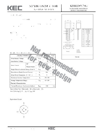
                                     SEMICONDUCTOR                                                     KHB1D0N70G
                                                                                                      N CHANNEL MOS FIELD
                                             TECHNICAL DATA                                            EFFECT TRANSISTOR

 General Description

   This planar stripe MOSFET has better characteristics, such as fast                          B                               C
 switching time, low on resistance, low gate charge and excellent
 avalanche characteristics. It is mainly suitable for switch mode power


                                                                                                                      A
 supplies and low power battery chargers.
                                                                                                                                   N   DIM   MILLIMETERS
                                                                                                                  E                     A     4.70 MAX
                                                                                       K
                                                                                                          G                             B     4.80 MAX
 FEATURES                                                                              D                                                C     3.70 MAX


                                                                                                                      J
                                                                                                                                        D        0.45
   VDSS= 700V, ID= 0.4A                                                                                                                 E        1.00
                                                                                                                                        F        1.27
   Drain-Source ON Resistance :                                                                                                         G        0.85
   RDS(ON)=9.0 (Typ.), @VGS = 10V                                                                                                       H        0.45
                                                                                                      H                                 J           _
                                                                                                                                              14.00 + 0.50
                                                                                       F                      F                         K     0.55 MAX
                                                                                                                                        L        2.30
                                                                                                                                        M     0.45 MAX
                                                                                                                                        N         1.00


                                                                                                                      C
                                                                                           1   2   3


                                                                                   L


                                                                                                                  M
                                                                                                                           1. GATE
                                                                                           * Bottom                        2. DRAIN
                                                                                                                           3. SOURCE
 MOSFET MAXIMUM RATING (Ta=25                         Unless otherwise noted)
             CHARACTERISTIC                       SYMBOL          RATING    UNIT
                                                                                                                          TO-92
   Drain-Source Voltage                              VDSS          700       V
   Gate-Source Voltage                               VGSS            30      V
                                DC                    ID            0.4      A
   Drain Current
                                Pulsed (Note1)        IDP           1.6      A
   Single Pulsed Avalanche Energy (Note 2)            EAS           25       mJ
   Drain-Source Diode Forward Current                  IS           0.4      A
   Drain Power Dissipation (TC=25       )             PD            3        W
   Maximum Junction Temperature                       Tj          -55~150
   Storage Temperature Range                          Tstg        -55~150
  Thermal Characteristics
   Thermal Resistance, Junction-to-Ambient           RthJA         120       /W

 Note 1) Pulse Test : Pulse width 10        , Duty cycle     1%
 Note 2) Starting Tj=25       , ID=1A, VDD=50V


 Equivalent Circuit

                          D


             G


                          S


2008. 5. 8                        Revision No : 2                                                                                                            1/6
                                                            KHB1D0N70G

 MOSFET ELECTRICAL CHARACTERISTICS (Ta=25                             Unless otherwise noted)
               CHARACTERISTIC                          SYMBOL                 TEST CONDITION          MIN.   TYP.   MAX.   UNIT

  Static
  Drain-Source Breakdown Voltage                         BVDSS        ID=250 A, VGS=0V                700     -       -     V
  Drain Cut-off Current                                   IDSS        VDS=700V, VGS=0V                 -      -     100     A
  Gate Leakage Current                                    IGSS        VGS=    30V, VDS=0V              -      -      100   nA
  Gate Threshold Voltage                                   Vth        VDS=VGS, ID=250 A                2      -      4      V
  Drain-Source ON Resistance                            RDS(ON)       VGS=10V, ID=0.5A                 -      9     10.5
  Forward Transconductance                                 gFS        VDS=15V, ID=0.5A                 -      1       -     S
  Dynamic
  Input Capacitance                                       Ciss                                         -     156      -
  Output Capacitance                                      Coss        VDS=25V, VGS=0V, f=1MHz          -     23.5     -     pF
  Reverse Transfer Capacitance                            Crss                                         -     3.8      -
  Total Gate Charge                                        Qg                                          -      7      9
  Gate-Source Charge                                       Qgs        VDS=560V, ID=1A, VGS=10V         -     1.1      -     nC
  Gate-Drain Charge                                       Qgd                                          -     3.7      -
  Turn-on Delay time                                      td(on)                                       -     6.5      -
  Turn-on Rise time                                         tr                                         -      10      -
                                                                      VDD=350V, ID=1A, RG=25                                ns
  Turn-off Delay time                                     td(off)                                      -      22      -
  Turn-off Fall time                                        tf                                         -      40      -


 ELECTRICAL CHARACTERISTICS (Ta=25                        Unless otherwise noted)

               CHARACTERISTIC                          SYMBOL                 TEST CONDITION          MIN.   TYP.   MAX.   UNIT
  Diode Forward Voltage                                   VDS         ISD=1A, VGS=0V                   -      -      1.4    V
  Reverse Recovery Time                                    Trr        VGS=0V, IS=1A, dIF/dt=100A/ s    -     140      -     ns

     Upper electrical characteristics can be changed because these are tentative specifications.
    Graphs are omitted because these are tentative specifications.


2008. 5. 8                         Revision No : 2                                                                                2/6
                                                                                                                   KHB1D0N70G


                                                                              Fig1. ID - VDS                                                                                                  Fig2. ID - VGS

                                                            VGS                                                                                                            VDS = 25V
                                                        TOP : 10.0 V
                                                                 6.0 V
                                                                 5.0 V
       Drain Current ID (A)


                                                                                                                           Drain Current ID (A)
                                                        Bottom : 4.5 V                                                                                             0
                                                   0                                                                                                          10
                                              10
                                                                                                                                                                           150 C


                                                                                                                                                                -1
                                                                                                                                                                            25 C                      -55 C
                                                   -1                                                                                                         10
                                              10


                                               -2                                                                                                               -2
                                              10                                                                                                              10
                                                        -1                         0                     1
                                                   10                         10                    10                                                                 2                 4            6             8               10

                                                                         Drain - Source Voltage VDS (V)                                                                             Gate - Source Voltage VGS (V)


                                                                            Fig3. BVDSS - Tj                                                                                                  Fig4. RDS(ON) - ID
         Normalized Breakdown Voltage BVDSS


                                              1.2                                                                                                             20
                                                                                                                                 On - Resistance RDS(ON) ()


                                                             VGS = 0V                                                                                                                                 VGS = 5V      VGS = 10V
                                                             IDS = 250


◦ Jabse Service Manual Search 2024 ◦ Jabse PravopisonTap.bg ◦ Other service manual resources online : FixyaeServiceinfo