Service Manuals, User Guides, Schematic Diagrams or docs for : . Electronic Components Datasheets Active components Transistors KEC khb9d0n90p1_f1

<< Back | Home

Most service manuals and schematics are PDF files, so You will need Adobre Acrobat Reader to view : Acrobat Download Some of the files are DjVu format. Readers and resources available here : DjVu Resources
For the compressed files, most common are zip and rar. Please, extract files with Your favorite compression software ( WinZip, WinRAR ... ) before viewing. If a document has multiple parts, You should download all, before extracting.
Good luck. Repair on Your own risk. Make sure You know what You are doing.


Image preview - the first page of the document
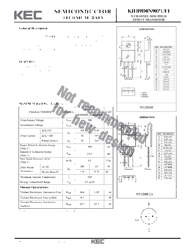
khb9d0n90p1_f1


>> Download khb9d0n90p1_f1 documenatation <<

Text preview - extract from the document
                                   SEMICONDUCTOR                                        KHB9D0N90P1/F1
                                                                                         N CHANNEL MOS FIELD
                                              TECHNICAL DATA                              EFFECT TRANSISTOR

  General Description                                                                        KHB9D0N90P1


    This planar stripe MOSFET has better characteristics, such as fast
  switching time, low on resistance, low gate charge and excellent
  avalanche characteristics. It is mainly suitable for electronic ballast and
  switching mode power supplies.


  FEATURES
    VDSS(Min.)= 900V, ID= 9A
    Drain-Source ON Resistance :
    RDS(ON)=1.4      @VGS =10V
    Qg(typ.) =75nC


  MAXIMUM RATING (Tc=25                   )
                                                                 RATING
              CHARACTERISTIC                  SYMBOL                             UNIT
                                                       KHB9D0N90P1 KHB9D0N90P1
                                                                                             KHB9D0N90F1
   Drain-Source Voltage                        VDSS                900            V
   Gate-Source Voltage                         VGSS                 30            V
                      @TC=25                               9.0           9.0*
                                                ID
   Drain Current      @TC=100                              36              36*    A
                      Pulsed (Note1)            IDP        36              36*
   Single Pulsed Avalanche Energy
                                               EAS                 900            mJ
   (Note 2)
   Repetitive Avalanche Energy
                                               EAR                20.5            mJ
   (Note 1)
   Peak Diode Recovery dv/dt
                                               dv/dt               4.5           V/ns
   (Note 3)
   Drain Power        Tc=25                               205              68     W
                                                PD
   Dissipation        Derate above25                      1.65           0.54    W/
   Maximum Junction Temperature                 Tj                 150
   Storage Temperature Range                   Tstg              -55 150
   Thermal Characteristics
   Thermal Resistance, Junction-to-Case        RthJC      0.61           1.85     /W
   Thermal Resistance, Case-to-Sink            RthCS       0.5              -     /W
   Thermal Resistance, Junction-to-
                                               RthJA      62.5           62.5     /W
   Ambient
  * : Drain current limited by maximum junction temperature.


2006. 5. 19                    Revision No : 0                                                                 1/7
                                                      KHB9D0N90P1/F1

 ELECTRICAL CHARACTERISTICS (Tc=25 )

               CHARACTERISTIC                         SYMBOL                 TEST CONDITION            MIN.   TYP.   MAX.   UNIT

   Static
   Drain-Source Breakdown Voltage                          BVDSS     ID=250 A, VGS=0V                  900     -       -     V
   Breakdown Voltage Temperature Coefficient           BVDSS/ Tj     ID=250 A, Referenced to 25         -     0.99     -    V/
   Drain Cut-off Current                                   IDSS      VDS=900V, VGS=0V                   -      -      10     A
   Gate Threshold Voltage                                   Vth      VDS=VGS, ID=250 A                 2.0     -      4.0    V
   Gate Leakage Current                                    IGSS      VGS=    30V, VDS=0V                -      -      100   nA
   Drain-Source ON Resistance                          RDS(ON)       VGS=10V, ID=4.5A                   -     1.12    1.4
   Dynamic
   Total Gate Charge                                        Qg                                          -      75     90
                                                                     VDS=720V, ID=9A
   Gate-Source Charge                                       Qgs                                         -      12      -     nC
                                                                     VGS=10V               (Note4,5)
   Gate-Drain Charge                                        Qgd                                         -     30.5     -
   Turn-on Delay time                                      td(on)                                       -      48    106
                                                                     VDD=4500V
   Turn-on Rise time                                         tr                                         -      70    150
                                                                     RL=25                                                   ns
   Turn-off Delay time                                     td(off)                                      -     289    588
                                                                     RG=9.0A               (Note4,5)
   Turn-off Fall time                                        tf                                         -     117    244
   Input Capacitance                                        Ciss                                        -     2663   3462
   Reverse Transfer Capacitance                             Crss     VDS=25V, VGS=0V, f=1.0MHz          -     183    238     pF
   Output Capacitance                                       Coss                                        -      20     26
   Source-Drain Diode Ratings
   Continuous Source Current                                 IS                                         -      -      8.0
                                                                     VGS


◦ Jabse Service Manual Search 2024 ◦ Jabse PravopisonTap.bg ◦ Other service manual resources online : FixyaeServiceinfo