Service Manuals, User Guides, Schematic Diagrams or docs for : . Electronic Components Datasheets Active components Transistors KEC kma2d8p20x

<< Back | Home

Most service manuals and schematics are PDF files, so You will need Adobre Acrobat Reader to view : Acrobat Download Some of the files are DjVu format. Readers and resources available here : DjVu Resources
For the compressed files, most common are zip and rar. Please, extract files with Your favorite compression software ( WinZip, WinRAR ... ) before viewing. If a document has multiple parts, You should download all, before extracting.
Good luck. Repair on Your own risk. Make sure You know what You are doing.


Image preview - the first page of the document
kma2d8p20x


>> Download kma2d8p20x documenatation <<

Text preview - extract from the document
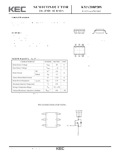
                                  SEMICONDUCTOR                                                                  KMA2D8P20X
                                             TECHNICAL DATA                                                      P-CH Trench MOSFET


  General Description

  It's mainly suitable for battery pack or power management in cell phone,
  and PDA.


                                                                                                                         D        H
  FEATURES
                                                                                                                                                             J
    VDSS=-20V, ID=-2.8A.                                                                                             E

    Drain-Source ON Resistance.
    : RDS(ON)=90m (Max.) @ VGS=-4.5V                                                                         A
                                                                                                                                      DIM   MILLIMETERS
                                                                                                                                       A           _
                                                                                                                                              3.00 + 0.15
    : RDS(ON)=150m (Max.) @ VGS=-2.5V                                                                    F                                          _
                                                                                                                                       B       1.65 + 0.1
                                                                                                                                       C            _
                                                                                                                                               2.85 + 0.2
    Super High Dense Cell Design for Extremely Low RDS(ON)
                                                                                                                                       D     1.0+0.15/-0.1
                                                                                                     6           4
                                                                                                                                       E        0~0.15
                                                                                                                         B    C        F       0.95 TYP
                                                                                                                                       G            _
                                                                                                                                               0.45 + 0.1
                                                                                                     1           3                     H           _
                                                                                                                                              0.15 + 0.05
                                                                                                                                       J      MIN 0.21

                                                                                                     G
  MAXIMUM RATING (Ta=25                  )
              CHARACTERISTIC                      SYMBOL     RATING               UNIT
   Drain-Source Voltage                            VDSS              -20                    V
                                                                                                                             TSOP-6
   Gate-Source Voltage                             VGSS         


◦ Jabse Service Manual Search 2024 ◦ Jabse PravopisonTap.bg ◦ Other service manual resources online : FixyaeServiceinfo