Service Manuals, User Guides, Schematic Diagrams or docs for : . Electronic Components Datasheets Active components Transistors KEC kma4d5p20x

<< Back | Home

Most service manuals and schematics are PDF files, so You will need Adobre Acrobat Reader to view : Acrobat Download Some of the files are DjVu format. Readers and resources available here : DjVu Resources
For the compressed files, most common are zip and rar. Please, extract files with Your favorite compression software ( WinZip, WinRAR ... ) before viewing. If a document has multiple parts, You should download all, before extracting.
Good luck. Repair on Your own risk. Make sure You know what You are doing.


Image preview - the first page of the document
kma4d5p20x


>> Download kma4d5p20x documenatation <<

Text preview - extract from the document
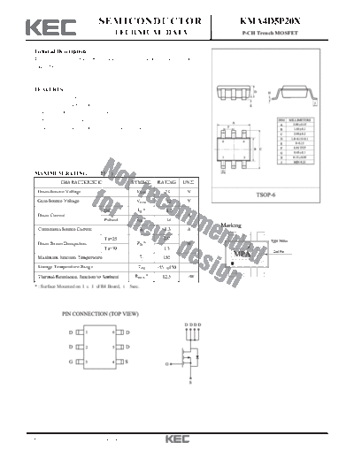
                                  SEMICONDUCTOR                               KMA4D5P20X
                                        TECHNICAL DATA                        P-CH Trench MOSFET


  General Description
  It s mainly suitable for battery pack or power management in cell phone,
  and PDA.


  FEATURES
    VDSS=-20V, ID=-4.5A.
    Drain-Source ON Resistance.
    : RDS(ON)=60m (Max.) @ VGS=-4.5V,.ID=-4.5A
    : RDS(ON)=110m (Max.) @ VGS=-2.5V,.ID=-3.3A
    Super High Dense Cell Design for Extremely Low RDS(ON)


  MAXIMUM RATING (Ta=25 )
              CHARACTERISTIC                     SYMBOL      RATING    UNIT
   Drain-Source Voltage                           VDSS         -20      V
   Gate-Source Voltage                            VGSS           12     V
                                   DC              ID *         4.5
   Drain Current                                                        A
                                   Pulsed          IDP*          16
   Continuous Source Current                        IS         -1.3     A
                                   Ta=25                       2.0
   Drain Power Dissipation                         PD *                 W
                                   Ta=70                       1.3
   Maximum Junction Temperature                     Tj         150
   Storage Temperature Range                       Tstg      -55 150
   Thermal Resistance, Junction to Ambient        RthJA *     62.5      /W
  * : Surface Mounted on 1   1 FR4 Board, t 5sec.


2007. 3. 22                    Revision No : 2                                                     1/5
                                                               KMA4D5P20X

 ELECTRICAL CHARACTERISTICS (Ta=25 )
                CHARACTERISTIC                      SYMBOL                      TEST CONDITION                  MIN.   TYP.   MAX.   UNIT
   Static
   Drain-Source Breakdown Voltage                    BVDSS          ID=-250 A, VGS=0V                           -20     -      -      V
                                                                    VGS=0V, VDS=-20V                             -      -      -1
   Drain Cut-off Current                                IDSS                                                                          A
                                                                    VGS=0V,VDS=-16V,       Tj=70        (Note    -      -      -5
   Gate Threshold Voltage                                Vth        VDS=VGS, ID=-250 A                          -0.6    -     -1.3    V
   Gate Leakage Current                                 IGSS        VGS=   12V, VDS=0V                           -      -      100   nA
                                                                    VGS=-4.5V, ID=-4.5A      (Note 2)            -      49     60
   Drain-Source ON Resistance                       RDS(ON)                                                                          m
                                                                    VGS=-2.5V, ID=-3.3A      (Note 2)            -      85    110
   Forward Transconductance                              gfs        VDS=-5V, ID=-4.5A      (Note 2)              -      7      -      S
   Dynamic    (Note 3)


   Total Gate Charge                                     Qg         VDS=-10V, RD=2.2                             -     8.5     -
   Gate-Source Charge                                    Qgs        VGS=-4.5V                                    -     1.8     -      nC
   Gate-Drain Charge                                    Qgd                                   (Fig.1)            -     2.9     -
   Turn-on Delay time                                   td(on)                                                   -      12     -
                                                                    VDS=-10V, RD=2.2
   Turn-on Rise time                                      tr                                                     -      32     -
                                                                    VGS=-4.5V RG=6                                                    ns
   Turn-off Delay time                                  td(off)                                                  -      64     -
                                                                                              (Fig.2)
   Turn-off Fall time                                     tf                                                     -      40     -
   Source-Drain Diode Ratings
   Continuous Source Current                              IS        VGS < Vth             (Note 1)               -      -     -1.3    A
   Diode Forward Voltage                                VSD         IS=-4.5A, VGS=0V      (Note 2)               -      -     -1.3    V
 Note 1) Based on thermal dissipation from junction to ambient while mounted on a 1        1 FR4 Board.
 Note 2) Pulse test : Pulse width 300    , Duty Cycle      2%
 Note 3) Guaranteed by design, not subject to production testing.


2007. 3. 22                       Revision No : 2                                                                                           2/5
                                KMA4D5P20X


2007. 3. 22   Revision No : 2                3/5
                                KMA4D5P20X


2007. 3. 22   Revision No : 2                4/5
                                KMA4D5P20X


2007. 3. 22   Revision No : 2                5/5


◦ Jabse Service Manual Search 2024 ◦ Jabse PravopisonTap.bg ◦ Other service manual resources online : FixyaeServiceinfo