Service Manuals, User Guides, Schematic Diagrams or docs for : . Electronic Components Datasheets Active components Transistors KEC kmb035n40db
<< Back | HomeMost service manuals and schematics are PDF files, so You will need Adobre Acrobat Reader to view : Acrobat Download Some of the files are DjVu format. Readers and resources available here : DjVu Resources
For the compressed files, most common are zip and rar. Please, extract files with Your favorite compression software ( WinZip, WinRAR ... ) before viewing. If a document has multiple parts, You should download all, before extracting.
Good luck. Repair on Your own risk. Make sure You know what You are doing.
Image preview - the first page of the document
>> Download kmb035n40db documenatation <<
Text preview - extract from the document
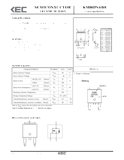
SEMICONDUCTOR KMB035N40DB
TECHNICAL DATA N-Ch Trench MOSFET
General Description
This Trench MOSFET has better characteristics, such as fast switching
time, low on resistance, low gate charge and excellent avalanche
characteristics. It is mainly suitable for Back-light Inverter and Power A K
L
DIM MILLIMETERS
C D A _
6.60 + 0.20
Supply. B _
6.10 + 0.20
C _
5.34 + 0.30
D _
0.70 + 0.20
B E _
2.70 + 0.15
F _
2.30 + 0.10
FEATURES G 0.96 MAX
H 0.90 MAX
VDSS=40V, ID=35A. H
J J _
1.80 + 0.20
E
Low Drain to Source On-state Resistance. G N K _
2.30 + 0.10
L _
0.50 + 0.10
: RDS(ON)=12.0m (Max.) @ VGS=10V F F M M _
0.50 + 0.10
N 0.70 MIN
: RDS(ON)=17.0m (Max.) @ VGS=4.5V O Max 0.1
1 2 3
O
MAXIMUM RATING ( )
CHARACTERISTIC SYMBOL N-Ch UNIT DPAK (1)
Drain to Source Voltage VDSS 40 V * Weight : 0.33g(typ)
Gate to Source Voltage VGSS 20 V
DC@TC=25 (Note1) ID 35
Drain Current A
Pulsed (Note2) IDP 140
@TC=25 (Note1) 43
Drain Power Dissipation PD W
@Ta=25 (Note2) 3.1
Maximum Junction Temperature Tj 150
Storage Temperature Range Tstg -55 150
Thermal Resistance, Junction to Case (Note1) RthJC 2.9 /W
Thermal Resistance, Junction to Ambient (Note2) RthJA 40 /W
Note 1) RthJC means that the infinite heat sink is mounted.
Note 2) Surface Mounted on 1 1 Pad of 2 oz copper.
PIN CONNECTION (TOP VIEW)
2009. 11. 9 Revision No : 1 1/2
KMB035N40DB
ELECTRICAL CHARACTERISTICS ( )
CHARACTERISTIC SYMBOL TEST CONDITION MIN. TYP. MAX. UNIT
Static
Drain to Source Breakdown Voltage BVDSS VGS=0V, ID=250 A 40 - - V
Drain Cut-off Current IDSS VGS=0V, VDS=32V - - 1 A
Gate to Source Leakage Current IGSS VGS= 20V, VDS=0V - - 100 nA
Gate to Source Threshold Voltage Vth VDS=VGS, ID=250 A 1.7 - 3.0 V
VGS=10V, ID=18A (Note3) - 8.0 12.0
Drain to Source On Resistance RDS(ON) m
VGS=4.5V, ID=16A (Note3) - 13.0 17.0
Forward Transconductance gfs VDS=5V, ID=18A (Note3) - 48 - S
Dynamic
Input Capacitance Ciss - 970 -
Ouput Capacitance Coss VDS=20V, f=1MHz, VGS=0V - 205 - pF
Reverse Transfer Capacitance Crss - 100 -
Gate Resistance Rg f=1MHz - 2.9 -
VGS=10V Qg - 20.2 -
Total Gate Charge
VGS=5V Qg - 10.7 -
VDS=20V, VGS=10V, ID=18A (Note3) nC
Gate to Source Charge Qgs - 5.1 -
Gate to Drain Charge Qgd - 4.6 -
Turn-On Delay Time td(on) - 18 -
Turn-On Rise Time tr VDD=20V, VGS=10V - 17 -
ns
Turn-Off Delay Time td(off) ID=18A, RG=6 (Note3) - 55 -
Turn-Off Fall Time tf - 13 -
Source-Drain Diode Ratings
Continuous Source Current IS - - 35 - A
Pulsed Source Current ISP - - 140 - A
Source to Drain Forward Voltage VSD VGS=0V, IS=3A (Note3) - 0.8 1.2 V
Reverse Recovery time trr IS=18A, dI/dt=100A/ S - 24 - ns
Reverse Recovered Charge Qrr IS=18A, dI/dt=100A/ S - 8.8 - nC
Note3) Pulse Test : Pulse width <300 , Duty cycle < 2%
2009. 11. 9 Revision No : 1 2/2
KMB035N40DB
2009. 11. 9 Revision No : 1 3/4
KMB035N40DB
2009. 11. 9 Revision No : 1 4/4
◦ Jabse Service Manual Search 2024 ◦ Jabse Pravopis ◦ onTap.bg ◦ Other service manual resources online : Fixya ◦ eServiceinfo