Service Manuals, User Guides, Schematic Diagrams or docs for : . Electronic Components Datasheets Active components Transistors KEC kmb3d5n40sa
<< Back | HomeMost service manuals and schematics are PDF files, so You will need Adobre Acrobat Reader to view : Acrobat Download Some of the files are DjVu format. Readers and resources available here : DjVu Resources
For the compressed files, most common are zip and rar. Please, extract files with Your favorite compression software ( WinZip, WinRAR ... ) before viewing. If a document has multiple parts, You should download all, before extracting.
Good luck. Repair on Your own risk. Make sure You know what You are doing.
Image preview - the first page of the document
>> Download kmb3d5n40sa documenatation <<
Text preview - extract from the document
SEMICONDUCTOR KMB3D5N40SA
TECHNICAL DATA N-Ch Trench MOSFET
General Description
This Trench MOSFET has better characteristics, such as fast switching
time, low on resistance, low gate charge and excellent avalanche
E
characteristics. It is mainly suitable for Load switch and Back-Light L B L
Inverter. DIM MILLIMETERS
A _
2.93 + 0.20
B 1.30+0.20/-0.15
C 1.30 MAX
D
2 3 D 0.40+0.15/-0.05
FEATURES
A
G
E 2.40+0.30/-0.20
H
1 G 1.90
VDSS=40V, ID=3.5A H 0.95
Drain-Source ON Resistance J 0.13+0.10/-0.05
K 0.00 ~ 0.10
RDS(ON)=45m (Max.) @ VGS=10V P P
L 0.55
M 0.20 MIN
RDS(ON)=62m (Max.) @ VGS=4.5V N 1.00+0.20/-0.10
N
C
Super High Dense Cell Design P 7
J
M
K
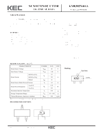
SOT-23
MAXIMUM RATING (Ta=25 )
CHARACTERISTIC SYMBOL N-Ch UNIT
Drain-Source Voltage VDSS 40 V
Gate-Source Voltage VGSS 20 V
DC@Ta=25 3.5
ID
Drain Current DC@Ta=70 2.8 A
Pulsed IDP 14
KN1
Drain-Source-Diode Forward Current IS 1.0 A
Ta=25 1.25
Drain Power Dissipation PD W
Ta=70 0.8
Maximum Junction Temperature Tj 150
Storage Temperature Range Tstg -55 150
Thermal Resistance, Junction to Ambient RthJA 100 /W
Note > *Surface Mounted on 1" 1" FR4 Board, t ◦ Jabse Service Manual Search 2024 ◦ Jabse Pravopis ◦ onTap.bg ◦ Other service manual resources online : Fixya ◦ eServiceinfo