Service Manuals, User Guides, Schematic Diagrams or docs for : . Electronic Components Datasheets Active components Transistors KEC kmb7d0dn40qa

<< Back | Home

Most service manuals and schematics are PDF files, so You will need Adobre Acrobat Reader to view : Acrobat Download Some of the files are DjVu format. Readers and resources available here : DjVu Resources
For the compressed files, most common are zip and rar. Please, extract files with Your favorite compression software ( WinZip, WinRAR ... ) before viewing. If a document has multiple parts, You should download all, before extracting.
Good luck. Repair on Your own risk. Make sure You know what You are doing.


Image preview - the first page of the document
kmb7d0dn40qa


>> Download kmb7d0dn40qa documenatation <<

Text preview - extract from the document
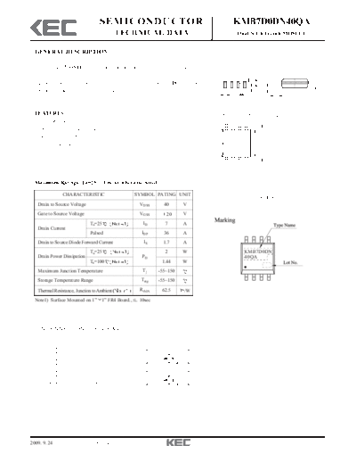
                                     SEMICONDUCTOR                                          KMB7D0DN40QA
                                              TECHNICAL DATA                                Dual N-Ch Trench MOSFET


  GENERAL DESCRIPTION

  This Trench MOSFET has better characteristics, such as fast switching
  time, low on resistance, low gate charge and excellent avalanche
  characteristics. It is mainly suitable for power management in PC, portable                               H
                                                                                                                T
  equipment and battery powered systems.                                                D       P       G                  L


  FEATURES                                                                                  A
                                                                                                                     DIM       MILLIMETERS
    VDSS=40V, ID=7A.                                                                                                  A               _
                                                                                                                                 4.85 + 0.2
                                                                                                                      B1              _
                                                                                                                                 3.94 + 0.2
    Drain to Source on Resistance.                                                                                    B2              _
                                                                                    8               5                            6.02 + 0.3
     RDS(ON)=25m     (Max.) @VGS=10V                                                                                  D               _
                                                                                                                                  0.4 + 0.1
                                                                                                            B1 B2     G        0.15+0.1/-0.05
     RDS(ON)=45m     (Max.) @VGS=4.5V                                                                                 H               _
                                                                                                                                 1.63 + 0.2
                                                                                    1               4                 L               _
                                                                                                                                 0.65 + 0.2
                                                                                                                      P             1.27
                                                                                                                      T        0.20+0.1/-0.05


  Maximum Ratings (Ta=25                  Unless otherwise noted)

                  CHARACTERISTIC                      SYMBOL PATING UNIT
                                                                                                             FLP-8
   Drain to Source Voltage                              VDSS        40     V
   Gate to Source Voltage                               VGSS         20    V
                                 Ta=25                    ID         7     A
   Drain Current
                                 Pulsed                  IDP        36     A
   Drain to Source Diode Forward Current                  IS        1.7    A
                                 Ta=25                               2     W                        KMB7D0DN
   Drain Power Dissipation                                PD                                        40QA
                                 Ta=100                             1.44   W
   Maximum Junction Temperature                           Tj     -55~150
   Storage Temperature Range                             Tstg    -55~150

   Thermal Resistance, Junction to Ambient               RthJA      62.5   /W
  Note1) Surface Mounted on 1" 1" FR4 Board., t


◦ Jabse Service Manual Search 2024 ◦ Jabse PravopisonTap.bg ◦ Other service manual resources online : FixyaeServiceinfo