Service Manuals, User Guides, Schematic Diagrams or docs for : . Electronic Components Datasheets Active components Transistors KEC kmb8d0p30qa

<< Back | Home

Most service manuals and schematics are PDF files, so You will need Adobre Acrobat Reader to view : Acrobat Download Some of the files are DjVu format. Readers and resources available here : DjVu Resources
For the compressed files, most common are zip and rar. Please, extract files with Your favorite compression software ( WinZip, WinRAR ... ) before viewing. If a document has multiple parts, You should download all, before extracting.
Good luck. Repair on Your own risk. Make sure You know what You are doing.


Image preview - the first page of the document
kmb8d0p30qa


>> Download kmb8d0p30qa documenatation <<

Text preview - extract from the document
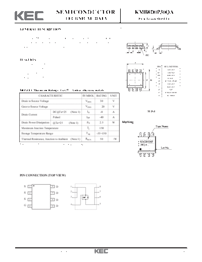
                                    SEMICONDUCTOR                                                      KMB8D0P30QA
                                            TECHNICAL DATA                                                 P-Ch Trench MOSFET


  GENERAL DESCRIPTION

   This Trench MOSFET has better characteristics, such as fast switching time, low
  on resistance, low gate charge and excellent avalanche characteristiscs. It is mainly
                                                                                                                       H
  suitable for Load Switch and Battery pack.
                                                                                                                           T
                                                                                                   D       P       G                 L
                                                                                                                       U

  FEATURES
                                                                                                       A
    VDSS=-30V, ID=-8A.
                                                                                                                               DIM       MILLIMETERS
    Drain to Source On Resistance.                                                                                              A                 _
                                                                                                                                             4.85 + 0.2
                                                                                                                                B1                _
                                                                                                                                             3.94 + 0.2
     RDS(ON)=20m (Max.) @ VGS=-10V                                                             8               5
                                                                                                                                B2                 _
                                                                                                                                             6.02 + 0.3
     RDS(ON)=35m (Max.) @ VGS=-4.5V                                                                                             D                 _
                                                                                                                                              0.4 + 0.1
                                                                                                                   B1 B2        G         0.15+0.1/-0.05
                                                                                               1                                H                  _
                                                                                                                                             1.63 + 0.2
                                                                                                               4
                                                                                                                                L                 _
                                                                                                                                             0.65 + 0.2
  MOSFET Maximum Ratings (Ta=25                      Unless otherwise noted)                                                    P               1.27
                                                                                                                                T         0.20+0.1/-0.05
                   CHARACTERISTIC                            SYMBOL RATING           UNIT                                       U            0.1 MAX

   Drain to Source Voltage                                     VDSS         30        V
   Gate to Source Voltage                                      VGSS             20    V
                                DC@Ta=25        (Note 1)           ID       -8        A                                FLP-8
   Drain Current
                                Pulsed                             IDP      -40       A
   Drain Power Dissipation      @Ta=25         (Note 1)            PD       2.5       W
   Maximum Junction Temperature                                    Tj      150
   Storage Temperature Range                                       Tstg   -55~150
   Thermal Resistance, Junction to Ambient      (Note 1)       RthJA        50            /W
                                                                                                               KMB8D0P
  Note1) Surface Mounted on 1        1 FR4 Board, t       10sec.                                               30QA


  PIN CONNECTION (TOP VIEW)


      S   1                    8    D           1                           8

                                                2                           7
      S   2                    7    D
                                                3                           6
      S   3                    6    D
                                                4                           5
      G   4                    5    D


2009. 6. 15                        Revision No : 0                                                                                                         1/4
                                                          KMB8D0P30QA

  ELECTRICAL CHARACTERISTICS (Ta=25 ) UNLESS OTHERWISE NOTED
              CHARACTERISTIC                 SYMBOL                 TEST CONDITION                MIN.   TYP.    MAX.   UNIT
   Static
   Drain to Source Breakdown Voltage           BVDSS       VGS=0V, ID=-250 A                      -30      -      -      V
   Drain Cut-off Current                        IDSS       VGS=0V, VDS=-24V                        -       -      -1     A
   Gate to Source Leakage Current               IGSS       VGS= 20V, VDS=0V                        -       -      100   nA
   Gate to Source Threshold Voltage              Vth       VDS=VGS, ID=-250 A                     -1.0     -     -3.0    V
                                                           VGS=-10V, ID=-8A             (Note2)    -      15      20
   Drain to Source On Resistance              RDS(ON)                                                                   m
                                                           VGS=-4.5V, ID=-5A            (Note2)    -      25      35
   Forward Transconductance                      gfs       VDS=-5V, ID=-8A              (Note2)    -      6       -      S
   Dynamic
   Input Capaclitance                           Ciss                                               -     1371     -
   Ouput Capacitance                            Coss       VDS=-15V, VGS=0V, f=1MHz     (Note2)    -     295      -      pF
   Reverse Transfer Capacitance                 Crss                                               -     176      -
                            VGS=10V                                                                -     28.2     -
   Total Gate Charge                             Qg
                            VGS=4.5V                                                               -     15.0     -
                                                           VDS=-15V, VGS=-10V, ID=-8A   (Note2)                          nC
   Gate to Source Charge                         Qgs                                               -     5.0      -
   Gate to Drain Charge                         Qgd                                                -     6.4      -
   Turn-On Delay Time                           td(on)                                             -     11.2     -
   Turn-On Rise Time                              tr       VDS=-15V, VGS=-10V                      -     5.8      -
                                                                                                                         ns
   Turn-Off Delay Time                          td(off)    ID=-8A, RG=1.6               (Note2)    -     65.0     -
   Turn-Off Fall Time                             tf                                               -     25.0     -
   Source to Drain Diode Ratings
   Source to Drain Forward Voltage              VSD        VGS=0V, IS=-1.7A             (Note2)    -     -0.75   -1.2    V

   Note2) Pulse Test : Pulse Width 300     , Duty Cycle   2%


2009. 6. 15                        Revision No : 0                                                                             2/4
                                KMB8D0P30QA


2009. 6. 15   Revision No : 0                 3/4
                                KMB8D0P30QA


2009. 6. 15   Revision No : 0                 4/4


◦ Jabse Service Manual Search 2024 ◦ Jabse PravopisonTap.bg ◦ Other service manual resources online : FixyaeServiceinfo