Service Manuals, User Guides, Schematic Diagrams or docs for : . Electronic Components Datasheets Active components Transistors KEC kra110-114

<< Back | Home

Most service manuals and schematics are PDF files, so You will need Adobre Acrobat Reader to view : Acrobat Download Some of the files are DjVu format. Readers and resources available here : DjVu Resources
For the compressed files, most common are zip and rar. Please, extract files with Your favorite compression software ( WinZip, WinRAR ... ) before viewing. If a document has multiple parts, You should download all, before extracting.
Good luck. Repair on Your own risk. Make sure You know what You are doing.


Image preview - the first page of the document
kra110-114


>> Download kra110-114 documenatation <<

Text preview - extract from the document
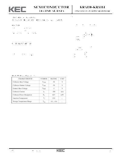
                                    SEMICONDUCTOR                                         KRA110~KRA114
                                            TECHNICAL DATA                    EPITAXIAL PLANAR PNP TRANSISTOR


  SWITCHING APPLICATION.
  INTERFACE CIRCUIT AND DRIVER CIRCUIT APPLICATION.
                                                                                          B                            C
  FEATURES
    With Built-in Bias Resistors.


                                                                                                              A
    Simplify Circuit Design.
    Reduce a Quantity of Parts and Manufacturing Process.
                                                                                                                            N   DIM   MILLIMETERS
                                                                                                          E                      A     4.70 MAX
                                                                                  K
                                                                                                  G                              B     4.80 MAX
                                                                                  D                                              C     3.70 MAX
                                                                                                                                 D        0.45


                                                                                                              J
                                                                                                                                 E        1.00
                                                                                                                                 F        1.27
  EQUIVALENT CIRCUIT
                                                                                                                                 G        0.85
                                                                                                                                 H        0.45
                                    C                                                         H                                  J           _
                                                                                                                                       14.00 + 0.50
                                                                                  F                   F                          K     0.55 MAX
                                                                                                                                 L        2.30
                 R1                                                                                                              M     0.45 MAX
     B                                                                                1   2   3
                                                                                                                                 N         1.00


                                                                                                          C
                                                                              L


                                                                                                      M
                                                                                                                  1. EMITTER
                                                                                                                  2. COLLECTOR
                                                                                                                  3. BASE
                                    E

                                                                                                                  TO-92


  MAXIMUM RATING (Ta=25                 )
              CHARACTERISTIC                SYMBOL      RATING      UNIT
   Collector-Base Voltage                     VCBO          -50           V
   Collector-Emitter Voltage                  VCEO          -50           V
   Emitter-Base Voltage                       VEBO           -5           V
   Collector Current                               IC       -100    mA
   Collector Power Dissipation                     PC       625     mW
   Junction Temperature                            Tj       150      


◦ Jabse Service Manual Search 2024 ◦ Jabse PravopisonTap.bg ◦ Other service manual resources online : FixyaeServiceinfo