Service Manuals, User Guides, Schematic Diagrams or docs for : . Electronic Components Datasheets Active components Transistors KEC kra119s

<< Back | Home

Most service manuals and schematics are PDF files, so You will need Adobre Acrobat Reader to view : Acrobat Download Some of the files are DjVu format. Readers and resources available here : DjVu Resources
For the compressed files, most common are zip and rar. Please, extract files with Your favorite compression software ( WinZip, WinRAR ... ) before viewing. If a document has multiple parts, You should download all, before extracting.
Good luck. Repair on Your own risk. Make sure You know what You are doing.


Image preview - the first page of the document
kra119s


>> Download kra119s documenatation <<

Text preview - extract from the document
                                    SEMICONDUCTOR                                                                      KRA119S
                                             TECHNICAL DATA                                         EPITAXIAL PLANAR PNP TRANSISTOR


  SWITCHING APPLICATION.
  INTERFACE CIRCUIT AND DRIVER CIRCUIT APPLICATION
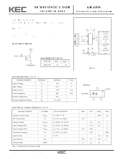
  FEATURES                                                                                                                      E
                                                                                                                       L        B           L
    With Built-in Bias Resistors.                                                                                                                    DIM   MILLIMETERS
                                                                                                                                                      A            _
                                                                                                                                                              2.93 + 0.20
    Simplify Circuit Design.                                                                                                                          B    1.30+0.20/-0.15
    Reduce a Quantity of Parts and Manufacturing Process.                                                                                             C       1.30 MAX


                                                                                                                                                D
                                                                                                                       2                    3         D    0.40+0.15/-0.05


                                                                                                      A

                                                                                                          G
                                                                                                                                                      E    2.40+0.30/-0.20


                                                                                                                  H
                                                                                                                       1                              G          1.90
                                                                                                                                                      H          0.95
  EQUIVALENT CIRCUIT                                                                                                                                  J    0.13+0.10/-0.05
                                                                                                                                                      K      0.00 ~ 0.10
                                                                                                     Q
                                                                                                                                                      L           0.55
                                                                                                                           P            P
                                                                                                                                                      M       0.20 MIN
                             OUT                                                                                                                      N    1.00+0.20/-0.10


                                                                                                                   N
                                                                                                              C
                                                                                                                                                      P            7


                                                                                                                                                J
                                                                                                                                                      Q         Max 0.1.
               R1


                                                                                                                           K
                                                                                                                                    M
     IN
                        R2                      BIAS RESISTOR VALUES
                                                      TYPE NO.       R1(k     )   R2(k   )

                      COMMON(+)                       KRA119S          4.7          10

                                                                                                                               SOT-23


  MAXIMUM RATING (Ta=25                  )
          CHARACTERISTIC                  SYMBOL                    RATING                   UNIT
  Output Voltage                                VO                    -50                     V
                                                                                                                  Marking
  Input Voltage                                 VI                   -25, 7                   V
                                                                                                                                                                   Lot No.
  Output Current                                IO                    -150                   mA
  Power Dissipation                             PD                    200                    mW           Type Name
                                                                                                                                        P6
  Junction Temperature                          Tj                    150
  Storage Temperature Range                  Tstg                   -55 150


  ELECTRICAL CHARACTERISTICS (Ta=25                            )

           CHARACTERISTIC                       SYMBOL             TEST CONDITION                         MIN.                 TYP.                 MAX.         UNIT

   Output Cut-off Current                            IO(OFF)       VO=-50V, VI=0                               -                 -                  -500           nA
   DC Current Gain                                     GI          VO=-5V, IO=-10mA                           30                 -                    -
   Output Voltage                                    VO(ON)        IO=-10mA, II=-0.5mA                         -               -0.1                 -0.3            V
   Input Voltage (ON)                                VI(ON)        VO=-0.3V, IO=-20mA                          -               -1.76                -2.5            V
   Input Voltage (OFF)                               VI(OFF)       VCC=-5V, IO=-100 A                     -0.3                 -0.82                  -             V

   Transition Frequency                               fT*          VO=-10V, IO=-5mA                            -               250                    -           MHz

   Input Current                                       II          VI=-5V                                      -                 -                  -1.8           mA
   Input Resistor                                     R1                             -                    3.29                 4.7                  6.11           k
   Resistor Ratio                                    R2/R1                           -                        1.7              2.1                   2.6

  Note : * Characteristic of Transistor Only.


2012. 8. 24                        Revision No : 0                                                                                                                           1/2
                                                                                          KRA119S


                                                   I O - V I(ON)                                                                                      I O - V I(OFF)
                              -100                                                                                         -3k
     OUTPUT CURRENT IO (mA)


                               -50


                                                                                                OUTPUT CURRENT I O (


◦ Jabse Service Manual Search 2024 ◦ Jabse PravopisonTap.bg ◦ Other service manual resources online : FixyaeServiceinfo