Service Manuals, User Guides, Schematic Diagrams or docs for : . Electronic Components Datasheets Active components Transistors KEC krc160f-164f

<< Back | Home

Most service manuals and schematics are PDF files, so You will need Adobre Acrobat Reader to view : Acrobat Download Some of the files are DjVu format. Readers and resources available here : DjVu Resources
For the compressed files, most common are zip and rar. Please, extract files with Your favorite compression software ( WinZip, WinRAR ... ) before viewing. If a document has multiple parts, You should download all, before extracting.
Good luck. Repair on Your own risk. Make sure You know what You are doing.


Image preview - the first page of the document
krc160f-164f


>> Download krc160f-164f documenatation <<

Text preview - extract from the document
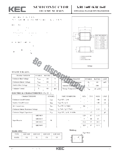
                                     SEMICONDUCTOR                                                                 KRC160F~KRC164F
                                             TECHNICAL DATA                                                EPITAXIAL PLANAR NPN TRANSISTOR


  SWITCHING APPLICATION.
  INTERFACE CIRCUIT AND DRIVER CIRCUIT APPLICATION.

  FEATURES
                                                                                                                                     E
    With Built-in Bias Resistors.
                                                                                                                                     B
    Simplify Circuit Design.
    Reduce a Quantity of Parts and Manufacturing Process.
    Thin fine Pitch Small Package.                                                                                     2                                   DIM       MILLIMETERS


                                                                                                       A
                                                                                                           G


                                                                                                                                                      D
                                                                                                                                                            A                _
                                                                                                                                                                         0.6 + 0.05
                                                                                                                                                3                            _


                                                                                                                   K
                                                                                                                                                            B            0.8 + 0.05
                                                                                                                       1                                    C         0.38+0.02/-0.04
                                                                                                                                                            D                _
                                                                                                                                                                         0.2 + 0.05
  EQUIVALENT CIRCUIT                                                                                                                                        E                _
                                                                                                                                                                         1.0 + 0.05
                                                                                                                                                            G                _
                                                                                                                                                                        0.35+ 0.05
                                    C                                                                                                                       J                _
                                                                                                                                                                         0.1 + 0.05
                                                                                                                                                            K                _
                                                                                                                                                                        0.15 + 0.05


                                                                                                               C
                R1


                                                                                                                                                      J
    B

                                                                                                                           1. COMMON (EMITTER)
                                                                                                                           2. IN (BASE)
                                                                                                                           3. OUT (COLLECTOR)
                                    E


                                                                                                                                         TFSM


  MAXIMUM RATING (Ta=25 )
         CHARACTERISTIC                 SYMBOL       RATING          UNIT
    Collector-Base Voltage                VCBO          20              V                 CHARACTERISTIC                             SYMBOL               RATING              UNIT
    Collector-Emitter Voltage             VCEO          20              V             Collector Power Dissipation                        PC                 50                 mW
    Emitter-Base Voltage                  VEBO          5               V             Junction Temperature                               Tj                 150
    Collector Current                        IC         50              mA            Storage Temperature Range                          Tstg             -55 150

  ELECTRICAL CHARACTERISTICS (Ta=25 )
                 CHARACTERISTIC                             SYMBOL                   TEST CONDITION                           MIN.         TYP.             MAX.              UNIT
    Collector Cut-off Current                                 ICBO               VCB=20V, IE=0                                   -               -          100                 nA
    Emitter Cut-off Current                                   IEBO               VEB=5V, IC=0                                    -               -          100                 nA
    DC Current Gain                                            hFE               VCE=5V, IC=1mA                                300               -               -
    Collector-Emitter Saturation Voltage                     VCE(sat)            IC=5mA, IB=0.25mA                               -               -          0.15                 V
    Collector Output Capacitance                               Cob               VCB=10V, IE=0, f=1MHz                           -              1.2              -              pF
                                        KRC160F                                                                                3.29             4.7         6.11
                                        KRC161F                                                                                  7              10           13
    Input Resistor                                             R1                               -                                                                              k
                                        KRC163F                                                                                15.4             22          28.6
                                        KRC164F                                                                                32.9             47          61.1


  MARK SPEC
                                                                                                    Marking
                                                                                                                               Type Name
        TYPE         KRC160F         KRC161F         KRC163F         KRC164F

      MARK              FK              FL             FN                   FP


2008. 11. 20                        Revision No :3                                                                                                                                      1/4
                                                                                       KRC160F~KRC164F


                                                                  IO - VI(ON)                                                                                          IO - VI(OFF)
                                         KRC160F                                                                                             KRC160F
                                  100                                                                                            10000
                                             VO= 0.2V                                                                                         VO= 5V
         OUTPUT CURRENT IO (mA)


                                                                                                       OUTPUT CURRENT IO (


◦ Jabse Service Manual Search 2024 ◦ Jabse PravopisonTap.bg ◦ Other service manual resources online : FixyaeServiceinfo