Service Manuals, User Guides, Schematic Diagrams or docs for : . Electronic Components Datasheets Active components Transistors KEC krc827u_829u
<< Back | HomeMost service manuals and schematics are PDF files, so You will need Adobre Acrobat Reader to view : Acrobat Download Some of the files are DjVu format. Readers and resources available here : DjVu Resources
For the compressed files, most common are zip and rar. Please, extract files with Your favorite compression software ( WinZip, WinRAR ... ) before viewing. If a document has multiple parts, You should download all, before extracting.
Good luck. Repair on Your own risk. Make sure You know what You are doing.
Image preview - the first page of the document
>> Download krc827u_829u documenatation <<
Text preview - extract from the document
SEMICONDUCTOR KRC827U~KRC829U
TECHNICAL DATA EPITAXIAL PLANAR NPN TRANSISTOR
SWITCHING APPLICATION.
INTERFACE CIRCUIT AND DRIVER CIRCUIT APPLICATION.
B
FEATURES B1
With Built-in Bias Resistors. 1 6 DIM MILLIMETERS
A _
2.00 + 0.20
C
Simplify Circuit Design. _
A1
2 5 A1 1.3 + 0.1
A
B _
2.1 + 0.1
C
Reduce a Quantity of Parts and Manufacturing Process.
3 4 D B1 _
1.25 + 0.1
High Packing Density. C 0.65
D 0.2+0.10/-0.05
G 0-0.1
H _
0.9 + 0.1
H
T T 0.15+0.1/-0.05
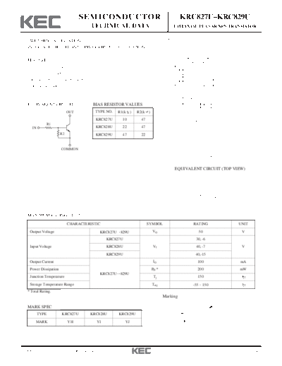
EQUIVALENT CIRCUIT BIAS RESISTOR VALUES
G
OUT TYPE NO. R1(k ) R2(k )
KRC827U 10 47 1. Q1 COMMON (EMITTER)
R1 2. Q2 COMMON (EMITTER)
IN KRC828U 22 47 3. Q2 IN (BASE)
4. Q2 OUT (COLLECTOR)
R2 KRC829U 47 22 5. Q1 IN (BASE)
6. Q1 OUT (COLLECTOR)
COMMON
US6
EQUIVALENT CIRCUIT (TOP VIEW)
6 5 4
Q1
Q2
1 2 3
MAXIMUM RATING (Ta=25 )
CHARACTERISTIC SYMBOL RATING UNIT
Output Voltage KRC827U 829U VO 50 V
KRC827U 30, -6
Input Voltage KRC828U VI 40, -7 V
KRC829U 40,-15
Output Current IO 100 mA
Power Dissipation PD * 200 mW
KRC827U 829U
Junction Temperature Tj 150
Storage Temperature Range Tstg -55 150
* Total Rating.
6 5 4
Marking
Lot No.
MARK SPEC
Type Name
TYPE KRC827U KRC828U KRC829U
MARK YH YI YJ
1 2 3
2008. 9. 23 Revision No : 2 1/4
KRC827U~KRC829U
ELECTRICAL CHARACTERISTICS (Ta=25 )
CHARACTERISTIC SYMBOL TEST CONDITION MIN. TYP. MAX. UNIT
Output Cut-off Current KRC827U 829U IO(OFF) VO=50V, VI=0 - - 500 nA
KRC827U 80 150 -
DC Current Gain KRC828U GI VO=5V, IO=10mA 80 150 -
KRC829U 70 140 -
Output Voltage KRC827U 829U VO(ON) IO=10mA, II=0.5mA - 0.1 0.3 V
KRC827U - 1.2 1.8
Input Voltage (ON) KRC828U VI(ON) VO=0.2V, IO=5mA - 1.8 2.6 V
KRC829U - 3.0 5.8
KRC827U 0.5 0.75 -
Input Votlage (OFF) KRC828U VI(OFF) VO=5V, IO=0.1mA 0.6 0.88 - V
KRC829U 1.5 1.82 -
Transition Frequency KRC827U 829U fT * VO=10V, IO=5mA - 200 - MHz
KRC827U - - 0.88
Input Current KRC828U II VI=5V - - 0.36 mA
KRC829U - - 0.16
KRC827U - 0.05 -
Rise
KRC828U tr - 0.12 -
Time
KRC829U - 0.26 -
KRC827U - 2.0 -
Switching Storage VO=5V, VIN=5V
KRC828U tstg - 2.4 - S
Time Time RL=1k
KRC829U - 1.5 -
KRC827U - 0.36 -
Fall
KRC828U tf - 0.4 -
Time
KRC829U - 0.41 -
Note : * Characteristic of Transistor Only.
2008. 9. 23 Revision No : 2 2/4
KRC827U~KRC829U
IO - VI(ON) IO - VI(OFF)
KRC827U KRC827U
50 3k
-25 25
OUTPUT CURRENT IO (◦ Jabse Service Manual Search 2024 ◦ Jabse Pravopis ◦ onTap.bg ◦ Other service manual resources online : Fixya ◦ eServiceinfo