Service Manuals, User Guides, Schematic Diagrams or docs for : . Electronic Components Datasheets Active components Transistors KEC pzta92

<< Back | Home

Most service manuals and schematics are PDF files, so You will need Adobre Acrobat Reader to view : Acrobat Download Some of the files are DjVu format. Readers and resources available here : DjVu Resources
For the compressed files, most common are zip and rar. Please, extract files with Your favorite compression software ( WinZip, WinRAR ... ) before viewing. If a document has multiple parts, You should download all, before extracting.
Good luck. Repair on Your own risk. Make sure You know what You are doing.


Image preview - the first page of the document
pzta92


>> Download pzta92 documenatation <<

Text preview - extract from the document
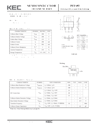
                                   SEMICONDUCTOR                                                                                 PZTA92
                                            TECHNICAL DATA                                        EPITAXIAL PLANAR PNP TRANSISTOR


  HIGH VOLTAGE APPLICATION.
                                                                                                                         A
  TELEPHONE APPLICATION.
                                                                                                                         H                             L
                                                                                                                             2

  FEATURES
    Complementary to PZTA42.
                                                                                                                                                            K
                                                                                              E    B


                                                                                                                1                        3
                                                                                                   J
  MAXIMUM RATING (Ta=25                 )
                                                                                                                                                 G
               CHARACTERISTIC               SYMBOL           RATING         UNIT                                    F            F


    Collector-Base Voltage                       VCBO            -300        V
                                                                                                            1            2           3           DIM        MILLIMETERS
                                                                                                                                                  A                _
                                                                                                                                                               6.5 + 0.2
    Collector-Emitter Voltage                    VCEO            -300        V                     C
                                                                                                                                                                   _
                                                                                                                                                 B             3.5 + 0.2

                                                 VEBO                                                                                            C                 1.8 MAX
    Emitter-Base Voltage                                         -5.0        V                                           D                       D               0.7+0.15/-0.1
                                                                                                                                                 E                    _
                                                                                                                                                                    7 + 0.3
    Collector Current                             IC             -500        mA
                                                                                                                                                 F                  2.3 TYP
                                                                                                                                                 G              0.26+0.09/-0.02
    Emitter Current                               IE             500         mA                   1. BASE
                                                                                                                                                 H               3.0+0.15/-0.1
                                                                                                  2. COLLECTOR (HEAT SINK)                                             _
                                                                                                                                                 J                1.75 + 0.25
    Collector Power Dissipation                  PC *              1         W                    3. EMITTER                                     K                0.1 MAX
                                                                                                                                                 L                10 MAX
    Junction Temperature                          Tj             150
    Storage Temperature                          Tstg        -55 150
   * Package Mounted On FR-4 PCB 36         18    1.5mm. :
                                                                                                                                     SOT-223
     mountina pad for the collector lead min.6cm2


                                                                                              Marking
                                                                                                       Type Name


                                                                                                                                 PZTA92
                                                                                                                                                           Lot No.


  ELECTRICAL CHARACTERISTICS (Ta=25                        )
                 CHARACTERISTIC                         SYMBOL                   TEST CONDITION                         MIN.             TYP.        MAX.                 UNIT
    Collector-Base Breakdown Voltage                    V(BR)CBO        IC=-100 A, IE=0                                 -300                 -              -                V
    Collector-Emitter Breakdown Voltage                 V(BE)CEO        IC=-1.0mA, IB=0                                 -300                 -              -                V
                                                                        IC=-1.0mA, VCE=-10V                              25                  -              -
    DC Current Gain                                      * hFE          IC=-10mA, VCE=-10V                               40                  -              -
                                                                        IC=-30mA, VCE=-10V                               25                  -              -
    Collector-Emitter Saturation Voltage                VCE(sat)        IC=-20mA, IB=-2.0mA                              -                   -         -0.5                  V
    Base-Emitter Saturation Voltage                     VBE(sat)        IC=-20mA, IB=-2.0mA                              -                   -         -0.9                  V
    Transition Frequency                                   fT           VCE=-20V, IC=-10mA, f=100MHz                     50                  -              -             MHz
    Collector Output Capacitance                          Cob           VCB=-20V, IE=0, f=1MHz                           -                   -             6.0               pF
   *Pulse Test : Pulse Width 300 S, Duty Cycle 2.0%


2004. 05. 21                      Revision No : 0                                                                                                                                 1/2
                                 PZTA92


2004. 05. 21   Revision No : 0            2/2


◦ Jabse Service Manual Search 2024 ◦ Jabse PravopisonTap.bg ◦ Other service manual resources online : FixyaeServiceinfo