Service Manuals, User Guides, Schematic Diagrams or docs for : . Electronic Components Datasheets Active components Transistors KEC 2n2906u

<< Back | Home

Most service manuals and schematics are PDF files, so You will need Adobre Acrobat Reader to view : Acrobat Download Some of the files are DjVu format. Readers and resources available here : DjVu Resources
For the compressed files, most common are zip and rar. Please, extract files with Your favorite compression software ( WinZip, WinRAR ... ) before viewing. If a document has multiple parts, You should download all, before extracting.
Good luck. Repair on Your own risk. Make sure You know what You are doing.


Image preview - the first page of the document
2n2906u


>> Download 2n2906u documenatation <<

Text preview - extract from the document
                                  SEMICONDUCTOR                                                    2N2906U
                                           TECHNICAL DATA              EPITAXIAL PLANAR PNP TRANSISTOR


  GENERAL PURPOSE APPLICATION.
  SWITCHING APPLICATION.

                                                                                            B
                                                                                            B1

  FEATURES
                                                                                   1                 6           DIM   MILLIMETERS
    Low Leakage Current                                                                                           A           _
                                                                                                                         2.00 + 0.20


                                                                               C
                                                                                                                              _


                                                                          A1
                                                                                   2                 5            A1      1.3 + 0.1


                                                                      A
      : ICEX=-50nA(Max.), IBL=-50nA(Max.)                                                                         B           _
                                                                                                                          2.1 + 0.1


                                                                           C
                                                                                   3                 4       D   B1            _
                                                                                                                          1.25 + 0.1
       @VCE=-30V, VEB=-3V.
                                                                                                                 C          0.65
    Excellent DC Current Gain Linearity.                                                                         D      0.2+0.10/-0.05
                                                                                                                 G          0-0.1
    Low Saturation Voltage                                                                                       H             _
                                                                                                                           0.9 + 0.1


                                                                               H
      : VCE(sat)=-0.4V(Max.) @IC=-50mA, IB=-5mA.                                                             T    T     0.15+0.1/-0.05

    Low Collector Output Capacitance                                                       G
      : Cob=4.5pF(Max.) @VCB=5V.
                                                                               1. Q 1   EMITTER
                                                                               2. Q 1   BASE
                                                                               3. Q 2   COLLECTOR
                                                                               4. Q 2   EMITTER
                                                                               5. Q 2   BASE
                                                                               6. Q 1   COLLECTOR


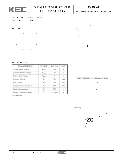
  MAXIMUM RATING (Ta=25                )
          CHARACTERISTIC                   SYMBOL    RATING    UNIT
                                                                                                    US6
   Collector-Base Voltage                    VCBO      -40      V
   Collector-Emitter Voltage                 VCEO      -40      V
   Emitter-Base Voltage                      VEBO      -5       V
                                               IC
                                                                          EQUIVALENT CIRCUIT (TOP VIEW)
   Collector Current                                  -200     mA
   Base Current                                IB      -50     mA                              6     5            4

   Collector Power Dissipation                PC       200     mW
   Junction Temperature                        Tj      150
                                                                                           Q1                     Q2
   Storage Temperature Range                  Tstg   -55 150
  * Total Rating

                                                                                               1     2            3


                                                                      Marking
                                                                                               6         5        4

                                                                                                                              Lot No.


                                                                                               ZC
                                                                      Type Name


                                                                                               1         2        3


2008. 9. 23                      Revision No : 1                                                                                         1/4
                                                             2N2906E

 ELECTRICAL CHARACTERISTICS (Ta=25 )
              CHARACTERISTIC                   SYMBOL                   TEST CONDITION                            MIN.    TYP.   MAX.    UNIT
   Collector Cut-off Current                        ICEX   VCE=-30V, VEB=-3V                                        -      -     -50     nA
   Base Cut-off Current                             IBL    VCE=-30V, VEB=-3V                                        -      -     -50     nA
   Collector-Base Breakdown Voltage            V(BR)CBO    IC=-10 A, IE=0                                         -40      -       -      V
   Collector-Emitter Breakdown Voltage *       V(BR)CEO    IC=-1mA, IB=0                                          -40      -       -      V
   Emitter-Base Breakdown Voltage              V(BR)EBO    IE=-10 A, IC=0                                         -5.0     -       -      V
                                                hFE(1)     VCE=-1V, IC=-0.1mA                                      60      -       -
                                                hFE(2)     VCE=-1V, IC=-1mA                                        80      -       -
   DC Current Gain                         *    hFE(3)     VCE=-1V, IC=-10mA                                      100      -     300
                                                hFE(4)     VCE=-1V, IC=-50mA                                       60      -       -
                                                hFE(5)     VCE=-1V, IC=-100mA                                      30      -       -
                                               VCE(sat)1   IC=-10mA, IB=-1mA                                        -      -     -0.25
   Collector-Emitter Saturation Voltage    *                                                                                              V
                                               VCE(sat)2   IC=-50mA, IB=-5mA                                        -      -     -0.4
                                               VBE(sat)1   IC=-10mA, IB=-1mA                                      -0.65    -     -0.85
   Base-Emitter Saturation Voltage         *                                                                                              V
                                               VBE(sat)2   IC=-50mA, IB=-5mA                                        -      -     -0.95
   Transition Frequency                              fT    VCE=-20V, IC=-10mA, f=100MHz                           250      -       -     MHz
   Collector Output Capacitance                     Cob    VCB=-5V, IE=0, f=1MHz                                    -      -      4.5     pF
   Input Capacitance                                Cib    VBE=-0.5V, IC=0, f=1MHz                                  -      -      10      pF
   Input Impedance                                  hie                                                           2.0      -      12     k
   Voltage Feedback Ratio                           hre                                                           1.0      -      10     x10-4
                                                           VCE=-10V, IC=-1mA, f=1kHz
   Small-Signal Current Gain                        hfe                                                           100      -     400
   Collector Output Admittance                      hoe                                                            3.0     -      60
                                                           VCE=-5V, IC=-0.1mA,
   Noise Figure                                     NF                                                              -      -      4.0     dB
                                                           Rg=1k       , f=10Hz 15.7kHz
                                                                                                         Vout

                            Delay Time               td                 10k                                         -      -      35
                                                                                                    C Total 4pF
                                                                                             275


                                                            V in


                                                             0.5V              0                 VCC =-3.0V
                            Rise Time                tr    -10.6V              t r ,t f < 1ns, Du=2%                -      -      35
                                                                      300ns
   Switching Time                                                                                                                         nS
                                                                                                        Vout

                            Storage Time            tstg              10k                                           -      -     225
                                                                                            275


                                                            V in                                    C Total 4pF
                                                                      1N916
                                                                   or equiv.
                                                                                                 VCC =-3.0V
                                                             9.1V              0
                            Fall Time                tf    -10.9V                                                   -      -      75
                                                                               t r ,t f < 1ns, Du=2%

                                                                       20


◦ Jabse Service Manual Search 2024 ◦ Jabse PravopisonTap.bg ◦ Other service manual resources online : FixyaeServiceinfo