Service Manuals, User Guides, Schematic Diagrams or docs for : . Electronic Components Datasheets Active components Transistors KEC 2n7002ka

<< Back | Home

Most service manuals and schematics are PDF files, so You will need Adobre Acrobat Reader to view : Acrobat Download Some of the files are DjVu format. Readers and resources available here : DjVu Resources
For the compressed files, most common are zip and rar. Please, extract files with Your favorite compression software ( WinZip, WinRAR ... ) before viewing. If a document has multiple parts, You should download all, before extracting.
Good luck. Repair on Your own risk. Make sure You know what You are doing.


Image preview - the first page of the document
2n7002ka


>> Download 2n7002ka documenatation <<

Text preview - extract from the document
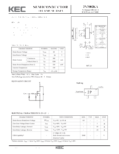
                                  SEMICONDUCTOR                                                                      2N7002KA
                                                                                                                    N Channel MOSFET
                                            TECHNICAL DATA                                                          ESD Protected 2000V

 INTERFACE AND SWITCHING APPLICATION.

 FEATURES                                                                                                                         E
                                                                                                                         L        B           L
   ESD Protected 2000V.
                                                                                                                                                      DIM    MILLIMETERS
   High density cell design for low RDS(ON).                                                                                                           A             _
                                                                                                                                                                2.93 + 0.20
                                                                                                                                                       B     1.30+0.20/-0.15
   Voltage controlled small signal switch.                                                                                                             C        1.30 MAX


                                                                                                                                                  D
                                                                                                                          2                   3        D     0.40+0.15/-0.05
   Rugged and reliable.


                                                                                                  A

                                                                                                        G
                                                                                                                                                       E     2.40+0.30/-0.20


                                                                                                                H
   High saturation current capablity.                                                                                     1                            G            1.90
                                                                                                                                                       H           0.95
                                                                                                                                                       J     0.13+0.10/-0.05
                                                                                                                                                       K       0.00 ~ 0.10
                                                                                                  Q
                                                                                                                                                       L            0.55
                                                                                                                              P           P
                                                                                                                                                       M        0.20 MIN
                                                                                                                                                       N     1.00+0.20/-0.10


                                                                                                                N
 MAXIMUM RATING (Ta=25                  )


                                                                                                            C
                                                                                                                                                       P             7


                                                                                                                                                  J
                                                                                                                                                       Q        0.1 MAX
             CHARACTERISTIC                      SYMBOL              RATING      UNIT


                                                                                                                              K
                                                                                                                                      M


   Drain-Source Voltage                               VDSS             60          V                                          1. SOURCE

   Gate-Source Voltage                                VGSS              20         V                                          2. GATE
                                                                                                                              3. DRAIN
                          Continuous                   ID              300
   Drain Current                                                                  mA
                          Pulsed (Note 1)             IDP             1200
   Drain Power Dissipation (Note 2)                   PD               350        mW
                                                                                                                                  SOT-23
   Junction Temperature                                Tj              150
   Storage Temperature Range                          Tstg           -55 150
 Note 1) Pulse Width 10      , Duty Cycle        1%
 Note 2) Package mounted on 99% Alumina 10 8                 0.6mm

 EQUIVALENT CIRCUIT
                                             D                                                        Marking

                                                                                                                                                             Lot No.


                   G
                                                                                                  Type Name
                                                                                                                                   2P


                                             S


 ELECTRICAL CHARACTERISTICS (Ta=25                               )

             CHARACTERISTIC                           SYMBOL                    TEST CONDITION                      MIN.              TYP.            MAX.          UNIT
   Drain-Source Breakdown Voltage                      BVDSS           VGS=0V, ID=10 A                               60                       -         -              V
   Zero Gate Voltage Drain Current                       IDSS          VDS=60V, VGS=0V                               -                        -         1               A
   Gate-Body Leakage, Forward                           IGSSF          VGS=20V, VDS=0V                               -                        -        10               A
   Gate-Body Leakage, Reverse                           IGSSR          VGS=-20V, VDS=0V                              -                        -        -10              A
                                                                       C=100pF, R=1.5K
   ESD-Capability*                                           -         Both forward and reverse                     2000                      -         -              V
                                                                       direction 3 pulse
 *Failure cirterion : IDSS > 1 A at VDS=60V, IGSSF>10 A at VGS=20V, IGSSR>-10 A at VGS=-20V.


2011. 4. 4                      Revision No : 1                                                                                                                                1/3
                                                                  2N7002KA

 ELECTRICAL CHARACTERISTICS (Ta=25 )
 ON CHARACTERISTICS (Note 3)
             CHARACTERISTIC                      SYMBOL                  TEST CONDITION        MIN.   TYP.   MAX.   UNIT
   Gate Threshold Voltage                             Vth         VDS=VGS, ID=250 A            1.1     -     2.35    V
                                                                  VGS=10V, ID=500mA             -      -      2.3
   Drain-Source ON Resistance                     RDS(ON)
                                                                  VGS=5V, ID=50mA               -     1.7     2.7
   Drain-Source Diode Forward Voltage                 VSD         VGS=0V, IS=200mA (Note 1)     -      -     1.15    V

 Note 3) Pulse Test : Pulse Width    80   , Duty Cycle       1%


 DYNAMIC CHARACTERISTICS
             CHARACTERISTIC                      SYMBOL                  TEST CONDITION        MIN.   TYP.   MAX.   UNIT
   Input Capacitance                                  Ciss                                      -     18.0     -
   Reverse Transfer Capacitance                       Crss        VDS=25V, VGS=0V, f=1          -     3.0      -     pF
   Output Capacitance                                 Coss                                      -     7.0      -
                        Turn-On Time                  ton         VDD=30V, RL=155 , ID=190 ,    -      15      -
   Switching Time                                                                                                    nS
                        Turn-Off Time                 toff        VGS=10V                       -      40      -


 SWITCHING TIME TEST CIRCUIT


2011. 4. 4                          Revision No : 1                                                                        2/3
                               2N7002KA


2011. 4. 4   Revision No : 1              3/3


◦ Jabse Service Manual Search 2024 ◦ Jabse PravopisonTap.bg ◦ Other service manual resources online : FixyaeServiceinfo