Service Manuals, User Guides, Schematic Diagrams or docs for : . Electronic Components Datasheets Active components Transistors Microsemi 2n6989-2n6990
<< Back | HomeMost service manuals and schematics are PDF files, so You will need Adobre Acrobat Reader to view : Acrobat Download Some of the files are DjVu format. Readers and resources available here : DjVu Resources
For the compressed files, most common are zip and rar. Please, extract files with Your favorite compression software ( WinZip, WinRAR ... ) before viewing. If a document has multiple parts, You should download all, before extracting.
Good luck. Repair on Your own risk. Make sure You know what You are doing.
Image preview - the first page of the document
>> Download 2n6989-2n6990 documenatation <<
Text preview - extract from the document
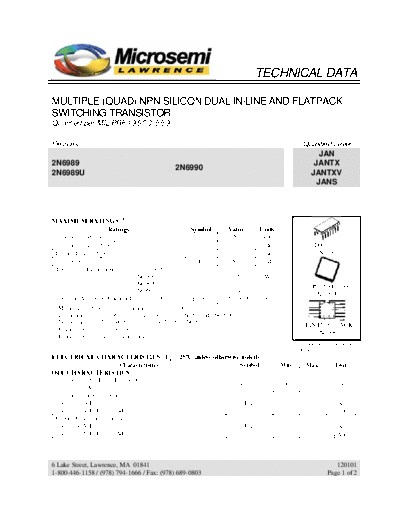
                                                                                 TECHNICAL DATA

MULTIPLE (QUAD) NPN SILICON DUAL IN-LINE AND FLATPACK
SWITCHING TRANSISTOR
Qualified per MIL-PRF-19500/559

Devices                                                                                            Qualified Level
                                                                                                        JAN
2N6989                                                                                                JANTX
                                              2N6990
2N6989U                                                                                              JANTXV
                                                                                                       JANS


MAXIMUM RATINGS (1)
             Ratings                                Symbol        Value          Units
 Collector-Emitter Voltage (3)                       VCEO          50              Vdc
 Collector-Base Voltage (3)                          VCBO          75              Vdc                  TO- 116*
 Emitter-Base Voltage (3)                            VEBO          6.0             Vdc                   2N6989
 Collector Current (3)                                IC           800             mAdc
 Total Power Dissipation        @ TA = +250C
                                2N6989(2)              PD           1.5             W
                                2N6989U(2)                          1.0                            20 PIN LEADLESS*
                                2N6990(2)                           0.4
                                                                                    0                   2N6989U
 Operating & Storage Junction Temperature Range       Top, Tstg -65 to +200         C
1) Maximum voltage between transistors shall be  500 Vdc
2) Derate linearly 8.57 mW/0C above TA = +250C for 2N6989 and 2N6989U
   Derate linearly 2.286 mW/0C above TA = +250C for 2N6990
                                                                                                 14 PIN FLAT PACK*
   Ratings apply to total package.
3) Ratings apply to each transistor in the array.                                                      2N6990
                                                                                                 *See appendix A for package
                                                                                                 outline
ELECTRICAL CHARACTERISTICS (TA = 250C unless otherwise noted)
                            Characteristics                             Symbol            Min.       Max.         Unit
OFF CHARACTERISTICS
 Collector-Emitter Breakdown Voltage
                                                                        V(BR)CEO           50                     Vdc
  IC = 10 mAdc
 Collector-Base Cutoff Current
  VCB = 60 Vdc                                                           ICBO                          10         Adc
  VCB = 75 Vdc; Ic= 10
◦ Jabse Service Manual Search 2024 ◦ Jabse Pravopis ◦ onTap.bg ◦ Other service manual resources online : Fixya ◦ eServiceinfo