Service Manuals, User Guides, Schematic Diagrams or docs for : . Electronic Components Datasheets Active components Transistors ST bdx53f

<< Back | Home

Most service manuals and schematics are PDF files, so You will need Adobre Acrobat Reader to view : Acrobat Download Some of the files are DjVu format. Readers and resources available here : DjVu Resources
For the compressed files, most common are zip and rar. Please, extract files with Your favorite compression software ( WinZip, WinRAR ... ) before viewing. If a document has multiple parts, You should download all, before extracting.
Good luck. Repair on Your own risk. Make sure You know what You are doing.


Image preview - the first page of the document
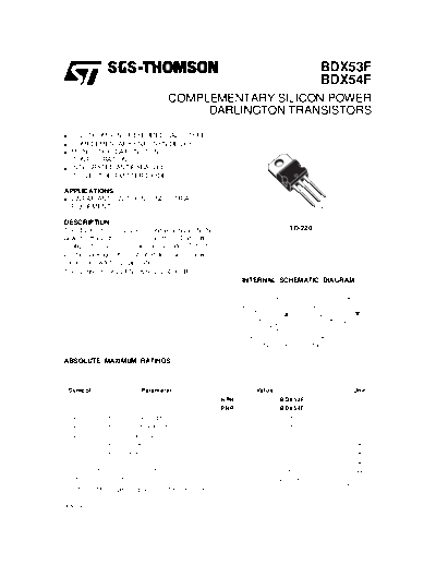
bdx53f


>> Download bdx53f documenatation <<

Text preview - extract from the document
                                                                                      BDX53F
                                                                                      BDX54F
                                       COMPLEMENTARY SILICON POWER
                                            DARLINGTON TRANSISTORS
s   SGS-THOMSON PREFERRED SALESTYPES
s   COMPLEMENTARY PNP - NPN DEVICES
s   MONOLITHIC DARLINGTON
    CONFIGURATION
s   INTEGRATED ANTIPARALLEL
    COLLECTOR-EMITTER DIODE

APPLICATIONS
s LINEAR AND SWITCHING INDUSTRIAL                                                         3
  EQUIPMENT                                                                           2
                                                                                  1

DESCRIPTION
The BDX53F is a silicon epitaxial-base NPN                               TO-220
power transistors in monolithic Darlington
configuration and are mounted in Jedec TO-220
plastic package. It is intented for use in power
linear and switching applications.
The complementary PNP types is BDX54F.
                                                         INTERNAL SCHEMATIC DIAGRAM


                                                            R1 Typ. = 10 K    R2 Typ. = 150 


ABSOLUTE MAXIMUM RATINGS


    Symbol                   Parameter                      Value                              Unit
                                                   NPN               BDX53F
                                                   PNP               BDX54F
     V CBO   Collector-Base Voltage (I E = 0)                           160                     V
     V CEO   Collector-Emitter Voltage (I B = 0)                        160                     V
     V EBO   Emitter-base Voltage (I C = 0)                              5                      V
      IC     Collector Current                                           8                      A
     I CM    Collector Peak Current                                     12                      A
      IB     Base Current                                               0.2                     A
     P tot   Total Dissipation at T c  25 C
                                          o
                                                                        60                      W
                                                                                               o
     T stg   Storage Temperature                                    -65 to 150                     C
                                                                                               o
      Tj     Max. Operating Junction Temperature                        150                        C

July 1997                                                                                              1/4
BDX53F / BDX54F

THERMAL DATA
                                                                                                            o
  R thj-case   Thermal Resistance Junction-case                                  Max          2.08              C/W
                                                                                                            o
  R thj-amb    Thermal Resistance Junction-ambient                               Max           70               C/W


ELECTRICAL CHARACTERISTICS (Tcase = 25 oC unless otherwise specified)


  Symbol               Parameter                            Test Conditions            Min.   Typ.   Max.   Unit
      I CEO    Collector Cut-off              V CB = 80 V                                            0.5    mA
               Current (I E = 0)
      I CBO    Collector Cut-off              V CB = 160 V                                           0.2    mA
               Current (I B = 0)
      I EBO    Emitter Cut-off Current        V EB = 5 V                                              5     mA
               (I C = 0)
 V CEO(sus)  Collector-Emitter                I C = 50 mA                              160                      V
             Sustaining Voltage
             (I B = 0)
  V CE(sat)    Collector-emitter              IC = 2 A              I B =10 mA                        2         V
               Saturation Voltage
  V BE(sat)    Base-emitter                   IC = 2 A              I B =10 mA                       2.5        V
               Saturation Voltage
      h FE     DC Current Gain                IC = 2 A              V CE = 5 V         500
                                              IC = 3 A              V CE = 5 V         150
      VF       Parallel Diode Forward         IF = 2 A                                               2.5        V
               Voltage
      hfe      Small Signal Current           I C = 0.5 A
               Gain                           f = 1MHz              V CE = 2 V                20
 Pulsed: Pulse duration = 300 


◦ Jabse Service Manual Search 2024 ◦ Jabse PravopisonTap.bg ◦ Other service manual resources online : FixyaeServiceinfo