Service Manuals, User Guides, Schematic Diagrams or docs for : . Electronic Components Datasheets Active components Transistors ST buld3n7t4
<< Back | HomeMost service manuals and schematics are PDF files, so You will need Adobre Acrobat Reader to view : Acrobat Download Some of the files are DjVu format. Readers and resources available here : DjVu Resources
For the compressed files, most common are zip and rar. Please, extract files with Your favorite compression software ( WinZip, WinRAR ... ) before viewing. If a document has multiple parts, You should download all, before extracting.
Good luck. Repair on Your own risk. Make sure You know what You are doing.
Image preview - the first page of the document
>> Download buld3n7t4 documenatation <<
Text preview - extract from the document
BULD3N7T4
Medium voltage fast-switching NPN Power Transistor
General features
Medium voltage capability
Low spread of dynamic parameters
Minimum lot-to-lot spread for reliable operation
Very high switching speed
In compliance with the 2002/93/EC European 3
Directive 1
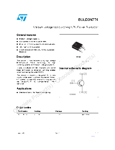
Description DPAK
t( s)
The device is manufactured using high voltage
Multi-Epitaxial Planar technology for high
d uc
switching speeds and medium voltage capability.
It uses a Cellular Emitter structure with planar
P ro
Internal schematic diagram
te
edge termination to enhance switching speeds
while maintaining the wide RBSOA.
le
so
The device is expressly designed for a new
solution to be used in compact fluorescent lamps,
Ob
H.F. ballast voltage FED where it is coupled with
the BULD3P5T4, its complementary PNP
transistor. -
Applications
ct (s)
du
Electronic ballast for fluorescent lighting
o
e Pr
let
so
Order codes
b
O Part Number
BULD3N7T4
Marking
BULD3N7
Package
DPAK
Packing
Tape & Reel
June 2006 Rev 1 1/10
www.st.com 10
BULD3N7T4
Contents
1 Electrical ratings . . . . . . . . . . . . . . . . . . . . . . . . . . . . . . . . . . . . . . . . . . . . 3
2 Electrical characteristics . . . . . . . . . . . . . . . . . . . . . . . . . . . . . . . . . . . . . 4
2.1 Electrical characteristics (curves) . . . . . . . . . . . . . . . . . . . . . . . . . . . . . . . . 5
2.2 Test circuits . . . . . . . . . . . . . . . . . . . . . . . . . . . . . . . . . . . . . . . . . . . . . . . . 6
3 Package mechanical data . . . . . . . . . . . . . . . . . . . . . . . . . . . . . . . . . . . . . 7
4 Revision history . . . . . . . . . . . . . . . . . . . . . . . . . . . . . . . . . . . . . . . . . . . . 9
t( s)
d uc
P ro
le te
so
- Ob
ct (s)
o du
e Pr
o let
O bs
2/10
BULD3N7T4 Electrical ratings
1 Electrical ratings
Table 1. Absolute maximum rating
Symbol Parameter Value Unit
VCES Collector-emitter voltage (V BE = 0) 700 V
VCEO Collector-emitter voltage (IB = 0) 400 V
Emitter-base voltage
VEBO V(BR)EBO V
(IC = 0, IB = 0.75 A, tp < 100ms, Tj < 150◦ Jabse Service Manual Search 2024 ◦ Jabse Pravopis ◦ onTap.bg ◦ Other service manual resources online : Fixya ◦ eServiceinfo