Service Manuals, User Guides, Schematic Diagrams or docs for : . Electronic Components Datasheets Active components Transistors ST st13003
<< Back | HomeMost service manuals and schematics are PDF files, so You will need Adobre Acrobat Reader to view : Acrobat Download Some of the files are DjVu format. Readers and resources available here : DjVu Resources
For the compressed files, most common are zip and rar. Please, extract files with Your favorite compression software ( WinZip, WinRAR ... ) before viewing. If a document has multiple parts, You should download all, before extracting.
Good luck. Repair on Your own risk. Make sure You know what You are doing.
Image preview - the first page of the document
>> Download st13003 documenatation <<
Text preview - extract from the document
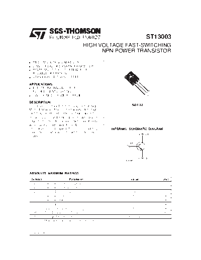
                                                                                ST13003
                                               HIGH VOLTAGE FAST-SWITCHING
                                                     NPN POWER TRANSISTOR
s   MEDIUM VOLTAGE CAPABILITY
s   LOW SPREAD OF DYNAMIC PARAMETERS
s   MINIMUM LOT-TO-LOT SPREAD FOR
    RELIABLE OPERATION
s   VERY HIGH SWITCHING SPEED

APPLICATIONS:
s ELECTRONIC BALLASTS FOR
  FLUORESCENT LIGHTING                                                              1
s SWITCH MODE POWER SUPPLIES                                                    2
                                                                            3

DESCRIPTION
The device is manufactured using high voltage                     SOT-32
Multi Epitaxial Planar technology for high
switching speeds and medium voltage capability.
It uses a Cellular Emitter structure with planar
edge termination to enhance switching speeds
while maintaining the wide RBSOA.
The device is designed for use in lighting             INTERNAL SCHEMATIC DIAGRAM
applications and low cost switch-mode power
supplies.


ABSOLUTE MAXIMUM RATINGS
    Symbol                        Parameter                      Value                  Uni t
     V CES    Collector-Emitter Voltage (V BE = 0)                700                    V
     V CEO    Collector-Emitter Voltage (I B = 0)                 400                    V
     V EBO    Emitter-Base Voltage (I C = 0)                       9                     V
      IC      Collector Current                                   1.5                    A
     I CM     Collector Peak Current (tp < 5 ms)                   3                     A
      IB      Base Current                                       0.75                    A
     I BM     Base Peak Current (t p < 5 ms)                      1.5                    A
     P t ot   Total Dissipation at T c = 25 o C                   40                     W
                                                                                         o
     T stg    St orage Temperature                             -65 to 150                    C
                                                                                         o
      Tj      Max. Operating Junction Temperature                 150                        C


January 1998                                                                                     1/7
ST13003

THERMAL DATA
                                                                                                                           o
  R t hj-ca se   Thermal Resistance Junction-case                                   Max                3.12                    C/W
                                                                                                                           o
      R thj-a    Thermal Resistance Junction-ambient                                Max                  89                    C/W


ELECTRICAL CHARACTERISTICS (Tcase = 25 oC unless otherwise specified)


  Symb ol              Parameter                           Test Cond ition s                 Min.      Typ .     Max.      Un it
      I CEV      Collector Cut-off           V CE = 700V                                                           1        mA
                 Current (V BE = -1.5V)      V CE = 700V                T j = 125 o C                              5        mA
      I EBO      Emitter Cut-off             V EB = 9 V                                                            1        mA
                 Current (IC = 0)
 V CEO(sus ) Collector-Emitter               I C = 10 mA                                      400                              V
             Sustaining Voltage              L = 25mH
             (I B = 0)
  V CE(sat )     Collector-Emitter           I C = 0.5 A                 I B = 0.1 A                              0.5          V
                 Saturation Voltage          IC = 1 A                    IB = 0.25 A                               1           V
                                             I C = 1.5 A                 I B = 0.5 A                               3           V
  V BE(s at)     Base-Emitter                I C = 0.5 A                 I B = 0.1 A                              1.0          V
                 Saturation Voltage          IC = 1 A                    IB = 0.25 A                              1.2          V
       h FE      DC Current G ain            I C = 0.5 A                 V CE = 2 V
                                             Group A                                           8                   20
                                             Group B                                          15                   35
                                             IC = 1 A                     V CE = 2 V           5                   25
                 RESISTIVE LO AD
        tr       Rise Time                   IC = 1 A                    V CC = 125 V                             1.0
◦ Jabse Service Manual Search 2024 ◦ Jabse Pravopis ◦ onTap.bg ◦ Other service manual resources online : Fixya ◦ eServiceinfo