Service Manuals, User Guides, Schematic Diagrams or docs for : . Electronic Components Datasheets Active components Transistors ST stw3040
<< Back | HomeMost service manuals and schematics are PDF files, so You will need Adobre Acrobat Reader to view : Acrobat Download Some of the files are DjVu format. Readers and resources available here : DjVu Resources
For the compressed files, most common are zip and rar. Please, extract files with Your favorite compression software ( WinZip, WinRAR ... ) before viewing. If a document has multiple parts, You should download all, before extracting.
Good luck. Repair on Your own risk. Make sure You know what You are doing.
Image preview - the first page of the document
>> Download stw3040 documenatation <<
Text preview - extract from the document
STW3040
High voltage fast-switching NPN power transistor
Features
.
High voltage capability
High DC current gain
Minimum lot-to-lot spread for reliable operation
Wide safe operating areas (forward and
reverse biased)
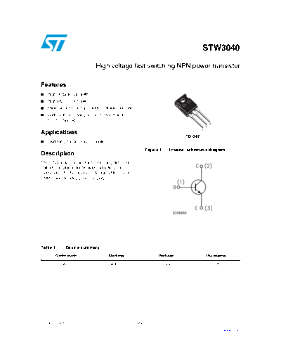
3
2
1
Applications
TO-247
Switching mode power supplies
Figure 1. Internal schematic diagram
Description
The STW3040 is manufactured using diffused
collector in planar technology adopting base
island layout. The device is designed for use in
SMPS and desktop power supply.
Table 1. Device summary
Order code Marking Package Packaging
STW3040 W3040 TO-247 Tube
October 2008 Rev 3 1/10
www.st.com 10
Absolute maximum ratings STW3040
1 Absolute maximum ratings
Table 2. Absolute maximum ratings
Symbol Parameter Value Unit
VCES Collector-emitter voltage (VCE = 0) 700 V
VCEO Collector-emitter voltage (IB = 0) 400 V
VEBO Emitter-base voltage (IC = 0) 9 V
IC Collector current 30 A
ICM Collector peak current 50 A
IB Base current 10 A
IBM Base peak current 15 A
PTOT Total dissipation at Tc = 25◦ Jabse Service Manual Search 2024 ◦ Jabse Pravopis ◦ onTap.bg ◦ Other service manual resources online : Fixya ◦ eServiceinfo