Service Manuals, User Guides, Schematic Diagrams or docs for : . Electronic Components Datasheets Active components Transistors ST stb11nk40z_stp11nk40zfp_stp11nk40z
<< Back | HomeMost service manuals and schematics are PDF files, so You will need Adobre Acrobat Reader to view : Acrobat Download Some of the files are DjVu format. Readers and resources available here : DjVu Resources
For the compressed files, most common are zip and rar. Please, extract files with Your favorite compression software ( WinZip, WinRAR ... ) before viewing. If a document has multiple parts, You should download all, before extracting.
Good luck. Repair on Your own risk. Make sure You know what You are doing.
Image preview - the first page of the document
>> Download stb11nk40z_stp11nk40zfp_stp11nk40z documenatation <<
Text preview - extract from the document
STB11NK40Z, STP11NK40ZFP
STP11NK40Z
N-channel 400 V, 0.49 9 A, TO-220, TO-220FP, D2PAK
,
Zener-protected SuperMESHTM Power MOSFET
Features
Type VDSS RDS(on) ID Pw
STB11NK40Z 400V <0.55 10A 110W
3
STP11NK40Z 400V <0.55 10A 110W 2
3
1
2
1
STP11NK40ZFP 400V <0.55 10A 30W
TO-220 TO-220FP
Extremely high dv/dt capability
100% avalanche tested 3
1
Gate charge minimized
D2PAK
Very low intrinsic capacitances
Very good manufacturing repeatability
Applications
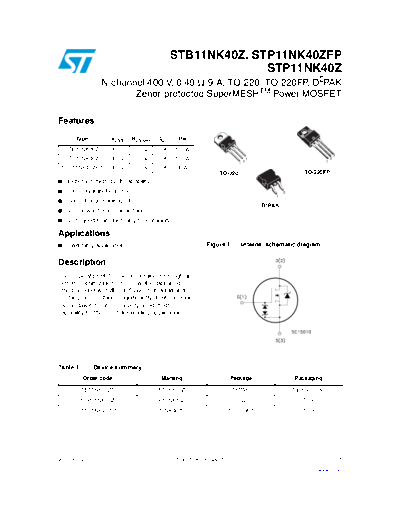
Switching application Figure 1. Internal schematic diagram
Description
The SuperMESHTM series is obtained through an
extreme optimization of ST's well established
strip-based PowerMESHTM layout. In addition to
pushing on-resistance significantly down, special
care is taken to ensure a very good dv/dt
capability for the most demanding applications.
Table 1. Device summary
Order code Marking Package Packaging
STB11NK40ZT4 B11NK40Z D◦ Jabse Service Manual Search 2024 ◦ Jabse Pravopis ◦ onTap.bg ◦ Other service manual resources online : Fixya ◦ eServiceinfo