Service Manuals, User Guides, Schematic Diagrams or docs for : . Electronic Components Datasheets Active components Transistors ST stb160nf02l
<< Back | HomeMost service manuals and schematics are PDF files, so You will need Adobre Acrobat Reader to view : Acrobat Download Some of the files are DjVu format. Readers and resources available here : DjVu Resources
For the compressed files, most common are zip and rar. Please, extract files with Your favorite compression software ( WinZip, WinRAR ... ) before viewing. If a document has multiple parts, You should download all, before extracting.
Good luck. Repair on Your own risk. Make sure You know what You are doing.
Image preview - the first page of the document
>> Download stb160nf02l documenatation <<
Text preview - extract from the document
STB160NF02L
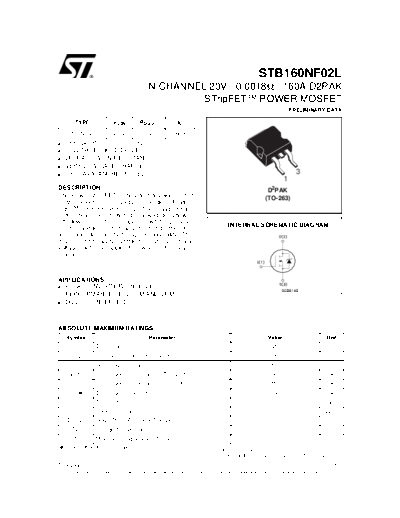
N-CHANNEL 20V - 0.0018 - 160A D2PAK
STripFETTM POWER MOSFET
PRELIMINARY DATA
TYPE VDSS RDS(on) ID
STB160NF02L 20 V < 0.0027 160 A
s TYPICAL RDS(on) = 0.0018
s LOW THRESHOLD DRIVE
s ULTRA LOW ON-RESISTANCE
s VERY LOW GATE CHARGE
s 100% AVALANCHE TESTED 3
1
DESCRIPTION D2PAK
This Power MOSFET is the latest development of (TO-263)
STMicroelectronics unique "Single Feature
SizeTM" strip-based process. The resulting tran-
sistor shows extremely high packing density with
ultra low on-resistance, superior switching charac-
INTERNAL SCHEMATIC DIAGRAM
teristics and less critical alignment steps therefore
a remarkable manufacturing reproducibility. This
device is particularly suitable for high current, low
voltage switching application where efficiency is
crucial.
APPLICATIONS
s BUCK CONVERTERS IN HIGH
PERFORMANCE TELECOM AND VRMs
s DC-DC CONVERTERS
ABSOLUTE MAXIMUM RATINGS
Symbol Parameter Value Unit
VDS Drain-source Voltage (VGS = 0) 20 V
VDGR Drain-gate Voltage (RGS = 20 k) 20 V
VGS Gate- source Voltage ◦ Jabse Service Manual Search 2024 ◦ Jabse Pravopis ◦ onTap.bg ◦ Other service manual resources online : Fixya ◦ eServiceinfo