Service Manuals, User Guides, Schematic Diagrams or docs for : . Electronic Components Datasheets Active components Transistors ST stb185n55f3_stp185n55f3
<< Back | HomeMost service manuals and schematics are PDF files, so You will need Adobre Acrobat Reader to view : Acrobat Download Some of the files are DjVu format. Readers and resources available here : DjVu Resources
For the compressed files, most common are zip and rar. Please, extract files with Your favorite compression software ( WinZip, WinRAR ... ) before viewing. If a document has multiple parts, You should download all, before extracting.
Good luck. Repair on Your own risk. Make sure You know what You are doing.
Image preview - the first page of the document
>> Download stb185n55f3_stp185n55f3 documenatation <<
Text preview - extract from the document
STB185N55F3
STP185N55F3
N-channel 55V - 3.2m - 120A - D2PAK/TO-220
STripFETTM Power MOSFET
Features
Type VDSS RDS(on) ID Pw
(1)
STB185N55F3 55V 3.5m 120A 330W
(1)
STP185N55F3 55V 3.8m 120A 330W
1. Value limited by wire bonding
3 3
Ultra low on-resistance 2 1
1
100% avalanche tested
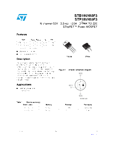
TO-220 D2PAK
Description
This n-channel enhancement mode Power
MOSFET is the latest refinement of
STMicroelectronics unique "single feature sizeTM"
strip-based process with less critical alignment Figure 1. Internal schematic diagram
steps and therefore a remarkable manufacturing
reproducibility. The resulting transistor shows
extremely high packing density for low on
resistance, rugged avalanche characteristics and
low gate charge.
Applications
Switching applications
◦ Jabse Service Manual Search 2024 ◦ Jabse Pravopis ◦ onTap.bg ◦ Other service manual resources online : Fixya ◦ eServiceinfo