Service Manuals, User Guides, Schematic Diagrams or docs for : . Electronic Components Datasheets Active components Transistors ST stb180n55f3_stp180n55f3
<< Back | HomeMost service manuals and schematics are PDF files, so You will need Adobre Acrobat Reader to view : Acrobat Download Some of the files are DjVu format. Readers and resources available here : DjVu Resources
For the compressed files, most common are zip and rar. Please, extract files with Your favorite compression software ( WinZip, WinRAR ... ) before viewing. If a document has multiple parts, You should download all, before extracting.
Good luck. Repair on Your own risk. Make sure You know what You are doing.
Image preview - the first page of the document
>> Download stb180n55f3_stp180n55f3 documenatation <<
Text preview - extract from the document
STB180N55F3
STP180N55F3
N-channel 55V - 3.2m - 120A - D2PAK/TO-220
STripFETTM Power MOSFET
Features
Type VDSS RDS(on) ID Pw
(1)
STB180N55F3 55V 3.5m 120A 330W
(1)
STP180N55F3 55V 3.8m 120A 330W
1. Value limited by wire bonding 3 3
2 1
1
Ultra low on-resistance
100% avalanche tested TO-220 D2PAK
Description
This n-channel enhancement mode Power
MOSFET is the latest refinement of
STMicroelectronics unique "single feature sizeTM"
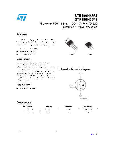
strip-based process with less critical alignment Internal schematic diagram
steps and therefore a remarkable manufacturing
reproducibility. The resulting transistor shows
extremely high packing density for low on
resistance, rugged avalanche characteristics and
low gate charge.
Application
Switching applications
Order codes
Part number Marking Package Packaging
2PAK
STB180N55F3 180N55F3 D Tape & reel
STP180N55F3 180N55F3 TO-220 Tube
June 2007 Rev 2 1/14
www.st.com 14
Contents STB180N55F3 - STP180N55F3
Contents
1 Electrical ratings . . . . . . . . . . . . . . . . . . . . . . . . . . . . . . . . . . . . . . . . . . . . 3
2 Electrical characteristics . . . . . . . . . . . . . . . . . . . . . . . . . . . . . . . . . . . . . 4
2.1 Electrical characteristics (curves) ............................. 6
3 Test circuit ................................................ 8
4 Package mechanical data . . . . . . . . . . . . . . . . . . . . . . . . . . . . . . . . . . . . . 9
5 Packaging mechanical data . . . . . . . . . . . . . . . . . . . . . . . . . . . . . . . . . . 12
6 Revision history . . . . . . . . . . . . . . . . . . . . . . . . . . . . . . . . . . . . . . . . . . . 13
2/14
STB180N55F3 - STP180N55F3 Electrical ratings
1 Electrical ratings
Table 1. Absolute maximum ratings
Symbol Parameter Value Unit
VDS Drain-source voltage (VGS=0) 55 V
VGS Gate-source voltage ◦ Jabse Service Manual Search 2024 ◦ Jabse Pravopis ◦ onTap.bg ◦ Other service manual resources online : Fixya ◦ eServiceinfo