Service Manuals, User Guides, Schematic Diagrams or docs for : . Electronic Components Datasheets Active components Transistors ST std17n05l_std17n06l

<< Back | Home

Most service manuals and schematics are PDF files, so You will need Adobre Acrobat Reader to view : Acrobat Download Some of the files are DjVu format. Readers and resources available here : DjVu Resources
For the compressed files, most common are zip and rar. Please, extract files with Your favorite compression software ( WinZip, WinRAR ... ) before viewing. If a document has multiple parts, You should download all, before extracting.
Good luck. Repair on Your own risk. Make sure You know what You are doing.


Image preview - the first page of the document
std17n05l_std17n06l


>> Download std17n05l_std17n06l documenatation <<

Text preview - extract from the document
                                                                                              STD17N05L
                                                                                              STD17N06L
                              N - CHANNEL ENHANCEMENT MODE
                       LOW THRESHOLD POWER MOS TRANSISTOR

        TYPE              VDSS          R DS(on)        ID
STD17N05L                 50 V        < 0.085          17 A
STD17N06L                 60 V        < 0.085          17 A

s   TYPICAL RDS(on) = 0.065 
s   AVALANCHE RUGGED TECHNOLOGY
s   100% AVALANCHE TESTED                                                                        3
s   REPETITIVE AVALANCHE DATA AT 100oC                                                       2                        3
    LOW GATE CHARGE                                                                      1
                                                                                                                s)
s
                                                                                                             1
    LOGIC LEVEL COMPATIBLE INPUT

                                                                                                             t(
s

s   175oC OPERATING TEMPERATURE

                                                                                                       uc
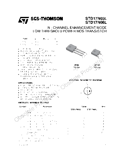
s   APPLICATION ORIENTED                                                    IPAK                          DPAK
    CHARACTERIZATION                                                       TO-251
                                                                                                     d    TO-252

                                                                                              ro
s   THROUGH-HOLE IPAK (TO-251) POWER                                     (Suffix "-1")                (Suffix "T4")
    PACKAGE IN TUBE (SUFFIX "-1")


                                                                             eP
s   SURFACE-MOUNTING DPAK (TO-252)


                                                                          let
    POWER PACKAGE IN TAPE & REEL
    (SUFFIX "T4")
                                                                       INTERNAL SCHEMATIC DIAGRAM
APPLICATIONS
                                                                       so
                                                                    Ob
s HIGH CURRENT, HIGH SPEED SWITCHING
s SOLENOID AND RELAY DRIVERS
  REGULATORS
                                                                  -
                                                    (s)
s

s DC-DC & DC-AC CONVERTERS


                                                 ct
s MOTOR CONTROL, AUDIO AMPLIFIERS
s AUTOMOTIVE ENVIRONMENT (INJECTION,

                                      du
  ABS, AIR-BAG, LAMPDRIVERS, Etc.)

                                    o
                        Pr
ABSOLUTE MAXIMUM RATINGS

    Symbol                             Parameter                                     Value                         Unit

                      e
               let
                                                                        STD17N05L                STD17N06L
     V DS      Drain-source Voltage (V GS = 0)                              50                       60                   V
             o
    bs
     V DGR     Drain- gate Voltage (R GS = 20 k)                            50                       60                   V
     V GS      Gate-source Voltage                                                       


◦ Jabse Service Manual Search 2024 ◦ Jabse PravopisonTap.bg ◦ Other service manual resources online : FixyaeServiceinfo