Service Manuals, User Guides, Schematic Diagrams or docs for : . Electronic Components Datasheets Active components Transistors ST stl20nm20n
<< Back | HomeMost service manuals and schematics are PDF files, so You will need Adobre Acrobat Reader to view : Acrobat Download Some of the files are DjVu format. Readers and resources available here : DjVu Resources
For the compressed files, most common are zip and rar. Please, extract files with Your favorite compression software ( WinZip, WinRAR ... ) before viewing. If a document has multiple parts, You should download all, before extracting.
Good luck. Repair on Your own risk. Make sure You know what You are doing.
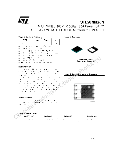
Image preview - the first page of the document

>> Download stl20nm20n documenatation <<
Text preview - extract from the document
                                                                               STL20NM20N
                    N-CHANNEL 200V - 0.088 - 20A PowerFLATTM
                 ULTRA LOW GATE CHARGE MDmeshTM II MOSFET

 Table 1: General Features                                 Figure 1: Package
       TYPE          VDSS        RDS(on)       ID

  STL20NM20N         200 V      < 0.105       20 A
    WORLDWIDE LOWEST GATE CHARGE
    TYPICAL RDS(on) = 0.088
    IMPROVED DIE-TO-FOOTPRINT RATIO
    VERY LOW PROFILE PACKAGE (1mm MAX)
    VERY LOW THERMAL RESISTANCE

                                                                                                    s)
    LOW GATE RESISTANCE
                                                                             PowerFlat (6x5)
    LOW INPUT CAPACITANCE                                                  (Chip Scale Package)
                                                                                                 t(
                                                                                        uc
    HIGH dv/dt and AVALANCHE CAPABILITIES

 DESCRIPTION
                                                                                      d
 This 200V MOSFET with a new advanced layout
 brings all unique advantages of MDmesh technol-
                                                                               P ro
                                                                       te
 ogy to lower voltages. The device exhibits world-         Figure 2: Internal Schematic Diagram
 wide lowest gate charge for any given on-
 resistance.Its use is therefore ideal as primary
                                                                    le
                                                          so
 switch in isolated DC-DC converters for Telecom
 and Computer applications.Used in combination


                                                       Ob
 with secondary-side low-voltage STripFETTM prod-
 ucts, it contributes to reducing losses and boosting
 efficiency.The new PowerFLATTM package allows
                                                     -
                                              s)
 a significant reduction in board space without com-

                                           t(
 promising performance.


 APPLICATIONS
                               d uc
                    ro
 The MDmeshTM family is very suitable for increas-

                   P
 ing power density allowing system miniaturization
 and higher efficiencies
                 e
      let
   so
 Table 2: Order Codes

Ob      SALES TYPE
       STL20NM20N
                                 MARKING
                                 L20NM20N
                                                           PACKAGE
                                                        PowerFLATTM(6x5)
                                                                                     PACKAGING
                                                                                     TAPE & REEL


                                                                                        Rev. 6
 January 2006                                                                                        1/10
STL20NM20N

 Table 3: Absolute Maximum ratings
   Symbol                                  Parameter                                      Value                   Unit
        VDS       Drain-source Voltage (VGS = 0)                                           200                     V
       VDGR       Drain-gate Voltage (RGS = 20 k)                                          200                     V
        VGS       Gate- source Voltage
◦ Jabse Service Manual Search 2024 ◦ Jabse Pravopis ◦ onTap.bg ◦ Other service manual resources online : Fixya ◦ eServiceinfo