Service Manuals, User Guides, Schematic Diagrams or docs for : . Electronic Components Datasheets Active components Transistors ST stl8nh3ll

<< Back | Home

Most service manuals and schematics are PDF files, so You will need Adobre Acrobat Reader to view : Acrobat Download Some of the files are DjVu format. Readers and resources available here : DjVu Resources
For the compressed files, most common are zip and rar. Please, extract files with Your favorite compression software ( WinZip, WinRAR ... ) before viewing. If a document has multiple parts, You should download all, before extracting.
Good luck. Repair on Your own risk. Make sure You know what You are doing.


Image preview - the first page of the document
stl8nh3ll


>> Download stl8nh3ll documenatation <<

Text preview - extract from the document
                                                                                    STL8NH3LL
                        N-channel 30 V, 0.012  8 A - PowerFLATTM (3.3x3.3)
                                               ,
                           ultra low gate charge STripFETTM Power MOSFET

Features
       Type             VDSS      RDS(on)       ID
    STL8NH3LL           30V       <0.015       8A (1)

    Improved die-to-footprint ratio
    Very low profile package (1mm max)
    Very low thermal resistance                                          PowerFLATTM(3.3x3.3)


    Very low gate charge
    Low threshold device
                                                                          (Chip Scale Package)


                                                                                                  t( s)
    In compliance with the 2002/95/EC European
    directive
                                                                                         d uc
Description                                                                    P ro
This application specific Power MOSFET is the
latest generation of STMicroelectronics unique
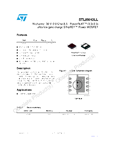
                                                          Figure 1.
                                                                         te
                                                                       Internal schematic diagram

                                                                      le
STripFETTM technology. The resulting transistor is
                                                             so
                                                          Ob
optimized for low on-resistance and minimal gate
charge. The chip-scaled PowerFLATTM package
allows a significant board space saving, still
                                                        -
                                         (s)
boosting the performance.

Applications
                                      ct
    Switching application
                               o du
                 e Pr                                                         TOP VIEW


        o let
   bs
Table 1.      Device summary

O          Order code

           STL8NH3LL
                                        Marking

                                            8NH3L
                                                                    Package

                                                            PowerFLATTM (3.3x3.3)
                                                                                            Packaging

                                                                                           Tape and reel


September 2009                                 Doc ID 10681 Rev 8                                          1/12
                                                                                                     www.st.com   12
 Contents                                                                                               STL8NH3LL


 Contents

 1          Electrical ratings . . . . . . . . . . . . . . . . . . . . . . . . . . . . . . . . . . . . . . . . . . . . 3

 2          Electrical characteristics . . . . . . . . . . . . . . . . . . . . . . . . . . . . . . . . . . . . . 4
            2.1      Electrical characteristics (curves)               ............................ 6

 3          Test circuits          .............................................. 8

 4          Package mechanical data . . . . . . . . . . . . . . . . . . . . . . . . . . . . . . . . . . . . . 9

 5          Revision history . . . . . . . . . . . . . . . . . . . . . . . . . . . . . . . . . . . . . . . . . . . 11


                                                                                                          t( s)
                                                                                                d uc
                                                                                     P ro
                                                                         le te
                                                          so
                                                     - Ob
                                       ct (s)
                            o du
                  e Pr
        o let
O bs


 2/12                                          Doc ID 10681 Rev 8
 STL8NH3LL                                                                                     Electrical ratings


 1           Electrical ratings

             Table 2.              Absolute maximum ratings
               Symbol                                       Parameter                      Value           Unit

                  VDS              Drain-source voltage (VGS = 0)                             30            V
                  VGS              Gate-source voltage                                        


◦ Jabse Service Manual Search 2024 ◦ Jabse PravopisonTap.bg ◦ Other service manual resources online : FixyaeServiceinfo