Service Manuals, User Guides, Schematic Diagrams or docs for : . Electronic Components Datasheets Active components Transistors ST stp14nf12
<< Back | HomeMost service manuals and schematics are PDF files, so You will need Adobre Acrobat Reader to view : Acrobat Download Some of the files are DjVu format. Readers and resources available here : DjVu Resources
For the compressed files, most common are zip and rar. Please, extract files with Your favorite compression software ( WinZip, WinRAR ... ) before viewing. If a document has multiple parts, You should download all, before extracting.
Good luck. Repair on Your own risk. Make sure You know what You are doing.
Image preview - the first page of the document
>> Download stp14nf12 documenatation <<
Text preview - extract from the document
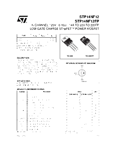
                                                                                         STP14NF12
                                                                                       STP14NF12FP
                       N-CHANNEL 120V - 0.16 - 14A TO-220/TO-220FP
                      LOW GATE CHARGE STripFETTM POWER MOSFET

        TYPE                VDSS         RDS(on)         ID

 STP14NF12                  120 V        < 0.18      14 A
 STP14NF12FP                120 V        < 0.18      14 A
s   TYPICAL RDS(on) = 0.16
s   EXCEPTIONAL dv/dt CAPABILITY
s   APPLICATION ORIENTED
                                                                                               3                              3
    CHARACTERIZATION                                                                       2                              2
                                                                                       1                              1


                                                                         TO-220                             TO-220FP
DESCRIPTION
This Power MOSFET series realized with STMicro-
electronics unique STripFET process has specifical-
                                                                       INTERNAL SCHEMATIC DIAGRAM
ly been designed to minimize input capacitance and
gate charge. It is therefore suitable as primary
switch in advanced high-efficiency isolated DC-DC
converters for Telecom and Computer application. It
is also intended for any application with low gate
charge drive requirements


APPLICATIONS
s HIGH-EFFICIENCY DC-DC CONVERTERS
s UPS AND MOTOR CONTROL


ABSOLUTE MAXIMUM RATINGS
    Symbol                                   Parameter                                         Value                      Unit
                                                                            STP14NF12                   STP14NF12FP
      VDS         Drain-source Voltage (VGS = 0)                                               120                         V
     VDGR         Drain-gate Voltage (RGS = 20 k)                                              120                         V
      VGS         Gate- source Voltage
◦ Jabse Service Manual Search 2024 ◦ Jabse Pravopis ◦ onTap.bg ◦ Other service manual resources online : Fixya ◦ eServiceinfo