Service Manuals, User Guides, Schematic Diagrams or docs for : . Electronic Components Datasheets Active components Transistors ST stp5nk90z_stf5nk90z

<< Back | Home

Most service manuals and schematics are PDF files, so You will need Adobre Acrobat Reader to view : Acrobat Download Some of the files are DjVu format. Readers and resources available here : DjVu Resources
For the compressed files, most common are zip and rar. Please, extract files with Your favorite compression software ( WinZip, WinRAR ... ) before viewing. If a document has multiple parts, You should download all, before extracting.
Good luck. Repair on Your own risk. Make sure You know what You are doing.


Image preview - the first page of the document
stp5nk90z_stf5nk90z


>> Download stp5nk90z_stf5nk90z documenatation <<

Text preview - extract from the document
                                                                               STP5NK90Z
                                                                               STF5NK90Z
                                  N-channel 900V - 2 - 4.5A - TO-220/TO-220FP
                                      Zener - Protected SuperMESHTM MOSFET

 General features
                    VDSS
      Type                     RDS(on)      ID    PW
                  (@Tjmax)
  STP5NK90Z         900 V      < 2.5      4.5 A   125W
  STF5NK90Z         900 V      < 2.5  4.5 A(1)    30W
                                                                                                        3
 1. Limited only by maximum temperature allowed                                                     2
                                                                                                1


                                                                                               s)
    Extremely high dv/dt capability
                                                                     TO-220          TO-220FP

                                                                                            t(
    Improved esd capability


                                                                                    uc
    100% avalanche rated
    Gate charge minimized
                                                                                  d


    Very low intrinsic capacitances
    Very good manufacturing repeatibility
                                                                              P ro
 Description                                                          te
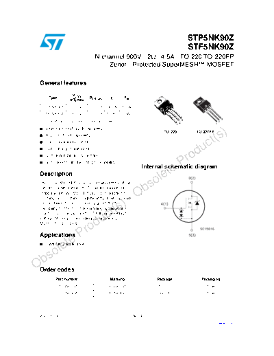
                                                             Internal schematic diagram
                                                                   le
 The SuperMESHTM series is obtained through an
                                                            so
                                                         Ob
 extreme optimization of ST's well established
 stripbased PowerMESHTM layout. In addition to
 pushing on-resistance significantly down, special
                                                       -
                                            (s)
 care is taken to ensure a very good dv/dt


                                         ct
 capability for the most demanding applications.
 Such series complements ST full range of high

                                 du
 voltage MOSFETs including revolutionary
 MDmeshTM products.
                               o
 Applications
                   e Pr
 
           let
    Switching application

         o
O bs
Order codes
          Part number                      Marking                Package              Packaging
          STP5NK90Z                        P5NK90Z                TO-220                 Tube
          STF5NK90Z                        F5NK90Z               TO-220FP                Tube


 August 2006                                             Rev 4                                              1/15
                                                                                                    www.st.com     15
 Contents                                                                              STP5NK90Z - STF5NK90Z


 Contents

 1          Electrical ratings . . . . . . . . . . . . . . . . . . . . . . . . . . . . . . . . . . . . . . . . . . . . 3
            1.1      Protection features of gate-to-source zener diodes . . . . . . . . . . . . . . . . . . 4

 2          Electrical characteristics . . . . . . . . . . . . . . . . . . . . . . . . . . . . . . . . . . . . . 5
            2.1      Electrical characteristics (curves)               ............................ 7

 3          Test circuit Package mechanical data . . . . . . . . . . . . . . . . . . . . . . . . . 10

 4          Package mechanical data . . . . . . . . . . . . . . . . . . . . . . . . . . . . . . . . . . . . 11


                                                                                                             s)
 5          Revision history . . . . . . . . . . . . . . . . . . . . . . . . . . . . . . . . . . . . . . . . . . . 14

                                                                                                          t(
                                                                                                d uc
                                                                                     P ro
                                                                         le te
                                                          so
                                                     - Ob
                                       ct (s)
                            o du
                  e Pr
        o let
O bs


 2/15
 STP5NK90Z - STF5NK90Z                                                                              Electrical ratings


 1        Electrical ratings

          Table 1.         Absolute maximum ratings
            Symbol                             Parameter                                   Value                    Unit

                                                                              STP5NK90Z          STF5NK90Z

               VDS          Drain-source voltage (VGS = 0)                                  900                      V
              VDGR          Drain-gate voltage (RGS = 20K)                                  900                      V
               VGS          Gate-source voltage                                            


◦ Jabse Service Manual Search 2024 ◦ Jabse PravopisonTap.bg ◦ Other service manual resources online : FixyaeServiceinfo