Service Manuals, User Guides, Schematic Diagrams or docs for : . Electronic Components Datasheets Active components Transistors ST stp85nf3ll_stb85nf3ll-1

<< Back | Home

Most service manuals and schematics are PDF files, so You will need Adobre Acrobat Reader to view : Acrobat Download Some of the files are DjVu format. Readers and resources available here : DjVu Resources
For the compressed files, most common are zip and rar. Please, extract files with Your favorite compression software ( WinZip, WinRAR ... ) before viewing. If a document has multiple parts, You should download all, before extracting.
Good luck. Repair on Your own risk. Make sure You know what You are doing.


Image preview - the first page of the document
stp85nf3ll_stb85nf3ll-1


>> Download stp85nf3ll_stb85nf3ll-1 documenatation <<

Text preview - extract from the document
                                                                              STP85NF3LL
                                                                             STB85NF3LL-1
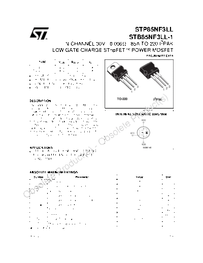
                           N-CHANNEL 30V - 0.006 - 85A TO-220/I2PAK
                       LOW GATE CHARGE STripFETTM POWER MOSFET
                                                                                              PRELIMINARY DATA

          TYPE               VDSS        RDS(on)         ID

     STP85NF3LL              30 V       < 0.008      85 A
     STB85NF3LL-1            30 V       < 0.008      85 A
 s    TYPICAL RDS(on) = 0.0075  (@4.5V)
 s    OPTIMAL RDS(ON) x Qg TRADE-OFF @4.5V
 s    CONDUCTION LOSSES REDUCED
      SWITCHING LOSSES REDUCED                                                       3                       3
                                                                                                          12
 s
                                                                                 2
                                                                             1


 DESCRIPTION
                                                                    TO-220
                                                                                                    t(
                                                                                                  I2PAK
                                                                                                       s)
                                                                                               uc
 This application specific Power MOSFET is the
 third genaration of STMicroelectronics unique "
 Single Feature Size" strip-based process. The re-
                                                                                             d
 sulting transistor shows the best trade-off between
 on-resistance and gate charge. When used as
 high and low side in buck regulators, it gives the
                                                                                   ro
                                                                   INTERNAL SCHEMATIC DIAGRAM

                                                                                 P
 best performance in terms of both conduction and
 switching losses. This is extremely important for
                                                                     le te
                                                                   so
 motherboards where fast switching and high effi-
 ciency are of paramount importance.


                                                              - Ob
                                                     (s)
 APPLICATIONS
 s SPECIFICALLY DESIGNED AND OPTIMISED


                                                  ct
   FOR HIGH EFFICIENCY CPU CORE DC/DC


                                      du
   CONVERTERS


                                    o
 ABSOLUTE MAXIMUM RATINGS

                       e Pr
                let
      Symbol                                 Parameter                               Value                 Unit
        VDS        Drain-source Voltage (VGS = 0)                                     30                    V

              o
  bs
       VDGR        Drain-gate Voltage (RGS = 20 k)                                    30                    V
        VGS        Gate- source Voltage                                              


◦ Jabse Service Manual Search 2024 ◦ Jabse PravopisonTap.bg ◦ Other service manual resources online : FixyaeServiceinfo