Service Manuals, User Guides, Schematic Diagrams or docs for : . Electronic Components Datasheets Active components Transistors ST stp9nc65
<< Back | HomeMost service manuals and schematics are PDF files, so You will need Adobre Acrobat Reader to view : Acrobat Download Some of the files are DjVu format. Readers and resources available here : DjVu Resources
For the compressed files, most common are zip and rar. Please, extract files with Your favorite compression software ( WinZip, WinRAR ... ) before viewing. If a document has multiple parts, You should download all, before extracting.
Good luck. Repair on Your own risk. Make sure You know what You are doing.
Image preview - the first page of the document
>> Download stp9nc65 documenatation <<
Text preview - extract from the document
STP9NC65
STP9NC65FP
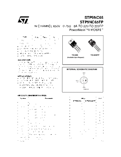
N-CHANNEL 650V - 0.75 - 8A TO-220/TO-220FP
PowerMeshTMII MOSFET
TYPE VDSS RDS(on) ID
STP9NC65 650 V < 0.90 8A
STP9NC65FP 650 V < 0.90 8A
s TYPICAL RDS(on) = 0.75
s EXTREMELY HIGH dv/dt CAPABILITY
3
s 100% AVALANCHE TESTED 2
1
s NEW HIGH VOLTAGE BENCHMARK
s GATE CHARGE MINIMIZED TO-220 TO-220FP
(Available Upon Request)
DESCRIPTION
The PowerMESHTMII is the evolution of the first
generation of MESH OVERLAYTM. The layout re-
finements introduced greatly improve the Ron*area
figure of merit while keeping the device at the lead-
INTERNAL SCHEMATIC DIAGRAM
ing edge for what concerns swithing speed, gate
charge and ruggedness.
APPLICATIONS
s HIGH CURRENT, HIGH SPEED SWITCHING
s SWITH MODE POWER SUPPLIES (SMPS)
s DC-AC CONVERTERS FOR WELDING
EQUIPMENT AND UNINTERRUPTIBLE
POWER SUPPLIES AND MOTOR DRIVES
ABSOLUTE MAXIMUM RATINGS
Symbol Parameter Value Unit
STP9NC65 STP9NC65FP
VDS Drain-source Voltage (VGS = 0) 650 V
VDGR Drain-gate Voltage (RGS = 20 k) 650 V
VGS Gate- source Voltage ◦ Jabse Service Manual Search 2024 ◦ Jabse Pravopis ◦ onTap.bg ◦ Other service manual resources online : Fixya ◦ eServiceinfo