Service Manuals, User Guides, Schematic Diagrams or docs for : . Electronic Components Datasheets Active components Transistors ST stsj25nf3ll

<< Back | Home

Most service manuals and schematics are PDF files, so You will need Adobre Acrobat Reader to view : Acrobat Download Some of the files are DjVu format. Readers and resources available here : DjVu Resources
For the compressed files, most common are zip and rar. Please, extract files with Your favorite compression software ( WinZip, WinRAR ... ) before viewing. If a document has multiple parts, You should download all, before extracting.
Good luck. Repair on Your own risk. Make sure You know what You are doing.


Image preview - the first page of the document
stsj25nf3ll


>> Download stsj25nf3ll documenatation <<

Text preview - extract from the document
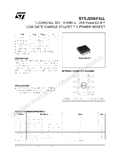
                                                                                           STSJ25NF3LL
                       N-CHANNEL 30V - 0.0085  - 25A PowerSO-8TM
                   LOW GATE CHARGE STripFETTM II POWER MOSFET

         TYPE               VDSS         RDS(on)        ID

     STSJ25NF3LL            30 V       <0.0105      25 A
 s    TYPICAL RDS(on) = 0.0085  @ 10V
 s    TYPICAL Qg = 24 nC @ 4.5 V
 s    CONDUCTION LOSSES REDUCED
 s    SWITCHING LOSSES REDUCED
 s    IMPROVED JUNCTION-CASE THERMAL
      RESISTANCE

 DESCRIPTION                                                                               PowerSO-8TM
                                                                                                            t( s)
                                                                                                          uc
 This Power MOSFET is the latest development of
 STMicroelectronics unique "Single Feature

                                                                                                        od
 SizeTM" strip-based process. This silicon, housed
 in thermally improved SO-8TM package, exhibits
                                                                                                      r
                                                                                    eP
 optimal on-resistance versus gate charge trade-                 INTERNAL SCHEMATIC DIAGRAM


                                                                                 et
 off plus lower R thj-c.


                                                                     ol
                                                                   bs
 APPLICATIONS
 s SPECIFICALLY DESIGNED AND OPTIMISED
                                                         ) -O
   FOR HIGH EFFICIENCY CPU CORE DC/DC
                                              t(s
                                           uc
   CONVERTERS FOR MOBILE PCS


                        ro               d                         DRAIN CONTACT ALSO ON THE BACKSIDE


             et       eP
          ol
  bs
 ABSOLUTE MAXIMUM RATINGS
      Symbol                            Parameter                                        Value                 Unit

O      VDS
       VDGR
                   Drain-source Voltage (VGS = 0)
                   Drain-gate Voltage (RGS = 20 k)
                                                                                           30
                                                                                           30
                                                                                                                V
                                                                                                                V
        VGS        Gate- source Voltage                                                   


◦ Jabse Service Manual Search 2024 ◦ Jabse PravopisonTap.bg ◦ Other service manual resources online : FixyaeServiceinfo