Service Manuals, User Guides, Schematic Diagrams or docs for : . Electronic Components Datasheets Active components Transistors ST vnd7n04_vnd7n04-1_vnk7n04fm
<< Back | HomeMost service manuals and schematics are PDF files, so You will need Adobre Acrobat Reader to view : Acrobat Download Some of the files are DjVu format. Readers and resources available here : DjVu Resources
For the compressed files, most common are zip and rar. Please, extract files with Your favorite compression software ( WinZip, WinRAR ... ) before viewing. If a document has multiple parts, You should download all, before extracting.
Good luck. Repair on Your own risk. Make sure You know what You are doing.
Image preview - the first page of the document
>> Download vnd7n04_vnd7n04-1_vnk7n04fm documenatation <<
Text preview - extract from the document
VND7N04, VND7N04-1
VNK7N04FM
"OMNIFET":
Fully autoprotected power MOSFET
Features
Type Vclamp RDS(on) Ilim
VND7N04 42 V 0.14 7A
VND7N04-1 42 V 0.14 7A
VNK7N04FM 42 V 0.14 7A
s Linear current limitation
s Thermal shut down
s Short circuit protection
s Integrated clamp
s Low current drawn from input pin
s Diagnostic feedback through input pin
s ESD protection
s Direct access to the gate of the power
MOSFET (analog driving) Description
s Compatible with standard power MOSFET
The VND7N04, VND7N04-1 and VNK7N04FM
are monolithic devices made using
STMicroeletronics VIPower M0 Technology,
intended for replacement of standard power
MOSFETS in DC to 50 KHz applications. Built-in
thermal shut-down, linear current limitation and
overvoltage clamp protect the chip in harsh
enviroments.
Fault feedback can be detected by monitoring the
voltage at the input pin.
Table 1. Device summary
Part number Order code
VND7N04, VND7N04-1-E,
VND7N04 VND7N04-E, VND7N0413TR,
VND7N04TR-E
VND7N04-1 VND7N04-1
VNK7N04FM VNK7N04FM
March 2009 Rev 1 1/17
www.st.com 17
Contents VND7N04, VND7N04-1, VNK7N04FM
Contents
1 Block diagram . . . . . . . . . . . . . . . . . . . . . . . . . . . . . . . . . . . . . . . . . . . . . . 3
2 Electrical specification . . . . . . . . . . . . . . . . . . . . . . . . . . . . . . . . . . . . . . . 4
2.1 Absolute maximum rating . . . . . . . . . . . . . . . . . . . . . . . . . . . . . . . . . . . . . . 4
2.2 Thermal data . . . . . . . . . . . . . . . . . . . . . . . . . . . . . . . . . . . . . . . . . . . . . . . 4
2.3 Electrical characteristics . . . . . . . . . . . . . . . . . . . . . . . . . . . . . . . . . . . . . . . 4
3 Protection features . . . . . . . . . . . . . . . . . . . . . . . . . . . . . . . . . . . . . . . . . . 7
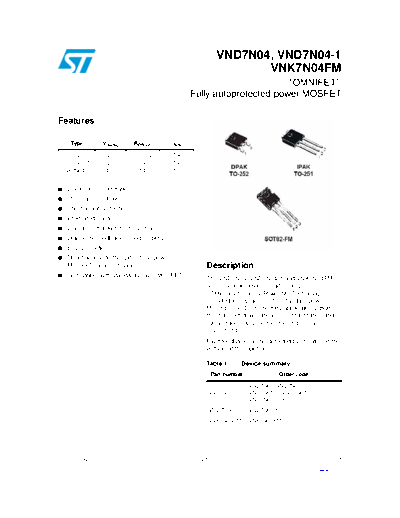
4 Package information . . . . . . . . . . . . . . . . . . . . . . . . . . . . . . . . . . . . . . . . 13
5 Revision history . . . . . . . . . . . . . . . . . . . . . . . . . . . . . . . . . . . . . . . . . . . 16
2/17
VND7N04, VND7N04-1, VNK7N04FM Block diagram
1 Block diagram
Figure 1. Block diagram
3/17
Electrical specification VND7N04, VND7N04-1, VNK7N04FM
2 Electrical specification
2.1 Absolute maximum rating
Table 2. Absolute maximum rating
Value
Symbol Parameter DPAK Unit
SOT-82FM
IPAK
VDS Drain-source voltage (Vin = 0) Internally clamped V
Vin Input voltage 18 V
ID Drain current Internally limited A
IR Reverse DC output current -7 A
Electrostatic discharge (C = 100 pF,
Vesd 2000 V
R=1.5 K)
Ptot Total dissipation at Tc = 25 ◦ Jabse Service Manual Search 2024 ◦ Jabse Pravopis ◦ onTap.bg ◦ Other service manual resources online : Fixya ◦ eServiceinfo