Service Manuals, User Guides, Schematic Diagrams or docs for : . Electronic Components Datasheets Active components Transistors Samsung ksc5021p
<< Back | HomeMost service manuals and schematics are PDF files, so You will need Adobre Acrobat Reader to view : Acrobat Download Some of the files are DjVu format. Readers and resources available here : DjVu Resources
For the compressed files, most common are zip and rar. Please, extract files with Your favorite compression software ( WinZip, WinRAR ... ) before viewing. If a document has multiple parts, You should download all, before extracting.
Good luck. Repair on Your own risk. Make sure You know what You are doing.
Image preview - the first page of the document
>> Download ksc5021p documenatation <<
Text preview - extract from the document
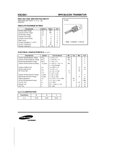
KSC5021                                                                        NPN SILICON TRANSISTOR
HIGH VOLTAGE AND HIGH RELIABILITY
HIGH SPEED SWITCHING : tf = 0.1       I (Typ)                                            TO-220
WIDE SOA

ABSOLUTE MAXIMUM RATINGS
             Characteristic                Symbol          Rating         Unit
 Collector-Base Voltage                    VCBO             800            V
 Collector-Emitter Voltage                 VCEO             500            V
 Emitter-Base Voltage                      VEBO                7           V
 Collector Current (DC)                    IC                  5           A
 Collector Current (Pulse)                 IC                10            A
 Base Current                              IB                  2           A
                              )
 Collector Dissipation ( T C=25            PC                50           W               1.Base 2.Collector 3.Emitter
 Junction Temperature                      TJ               150
 Storage Temperature                       T STG          -55 ~ 150

ELECTRICAL CHARACTERISTICS (Tc =25)
             Characteristic                 Symbol                  Test Conditions          Min      Typ   Max      Unit
 Collector Base Breakdown Voltage          BVCBO            IC = 1mA, IE = 0                  800                        V
 Collector Emitter Breakdown Voltage       BVCEO            IC = 5mA, RBE =                   500                        V
 Emitter Base Breakdown Voltage            BVEBO            IE = 1mA, IC = 0                      7                      V
 Collector Emitter Sustaining Voltage      VCEX(sus)        IC = 2.5A, IB1 = -IB2 = 1A        500                        V
                                                            L = 1mH, Clamped
 Collector Cutoff Current                  ICBO             VCB = 500V, IE = 0                               10      uA
 Emitter Cutoff Current                    IEBO             VEB = 5V, IC = 0                                 10      uA
 DC Current Gain                           hFE1             VCE = 5V, IC = 0.6A                15             50
                                           hFE2             VCE = 5V, IC = 3A                     8
 Collector Emitter Saturation Voltage      VCE(sat)         IC = 3A, IB = 0.6A                                 1         V
 Base Emitter Saturation Voltage           VBE(sat)         IC = 3A, IB = 0.6A                               1.5         V
 Output Capacitance                        COB              VCB = 10V, IE = 0, f = 1MHz               80             pF
 Current Gain Bandwidth Product            fT               VCE = 10V, IC = 0.6A                      18             MHz
 Turn On Time                              tON              VCC = 200V                                       0.5     uS
 Storage Time                              tS               5IB1 = -2.5IB2 = IC = 4A                           3     uS
 Fall Time                                 tF               RL = 50
◦ Jabse Service Manual Search 2024 ◦ Jabse Pravopis ◦ onTap.bg ◦ Other service manual resources online : Fixya ◦ eServiceinfo