Service Manuals, User Guides, Schematic Diagrams or docs for : . Electronic Components Datasheets Active components Transistors Secos 2sb1119-1619

<< Back | Home

Most service manuals and schematics are PDF files, so You will need Adobre Acrobat Reader to view : Acrobat Download Some of the files are DjVu format. Readers and resources available here : DjVu Resources
For the compressed files, most common are zip and rar. Please, extract files with Your favorite compression software ( WinZip, WinRAR ... ) before viewing. If a document has multiple parts, You should download all, before extracting.
Good luck. Repair on Your own risk. Make sure You know what You are doing.


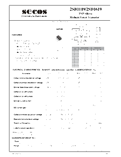
Image preview - the first page of the document
2sb1119-1619


>> Download 2sb1119-1619 documenatation <<

Text preview - extract from the document
                                                                                        2SB1119/2SD1619
                                                                                              PNP Silicon
                 Elektronische Bauelemente
                                                                                        Medium Power Transistor
                                                         RoHS Compliant Product
                                                                                                                     D

                                                                                                                    D1
                                                                                                                                                                      A


                                                                 SOT-89


                                                                                         E1


                                                                                                                                                 E
  FEATURES                                                                                                                     b1


      Power dissipation                                                                                        e
                                                                                                                                         b
                                                                                                                                                       C


                                                                                              L
        P CM : 500mW Tamb=25                                                                                         e1

                                                    1.BASE
      Collector current
                                                    2.COLLECTOR                                                      Dimensions In Millimeters              Dimensions In Inches
                                                                                                  Symbol
        ICM : -1        A
                                                    3.EMITTER
                                                                                                                   Min                  Max           Min                     Max
                                                                                                  A                1.400                1.600         0.055                   0.063
      Collector-base voltage                                                                      b                0.320                0.520         0.013                   0.020
                                                                                                  b1               0.360                0.560         0.014                   0.022
        VB(BR)CBO : -25     V                                                                     c                0.350                0.440         0.014                   0.017
                                                                                                  D                4.400                4.600         0.173                   0.181
      Operating and storage junction temperature range                                            D1               1.400                1.800         0.055                   0.071
                                                                                                  E                2.300                2.600         0.091                   0.102
        TJ Tstg: -55 to +150                                                                      E1               3.940                4.250         0.155                   0.167
                                                                                                  e                          1.500TYP                             0.060TYP
                                                                                                  e1               2.900                3.100         0.114                   0.122
                                                                                                  L                0.900                1.100         0.035                   0.043


   ELECTRICAL CHARACTERISTICS           Tamb=25          unlessotherwise         specified CLASSIFICATION OF                                          hFE(1)

                  Parameter                  Symbol                Test      conditions                    MIN                  TYP                  MAX                  UNIT

     Collector-base breakdown voltage       V(BR)CBO             Ic=-10 A        IE=0                       -25                                                              V

     Collector-emitter breakdown voltage    V(BR)CEO             IC= -1 mA , IB=0                           -25                                                              V

     Emitter-base breakdown voltage         V(BR)EBO             IE= -10     A   IC=0                        -5                                                              V

     Collector cut-off current              ICBO                 VCB= -20 V ,     IE=0                                                               -0.1                      A

     Collector cut-off current              ICEO                 VCE= -20 V , IB=0                                                                   -0.1                      A

     Emitter cut-off current                IEBO                 VEB=-4V ,       IC=0                                                                -0.1                      A

                                            hFE    1             VCE= -2V, IC= -50mA                       100                                       560
     DC current gain
                                            hFE    2             VCE=-2V, IC= -1A                           40

     Collector-emitter saturation voltage   VCE(sat)             IC=-0.5A,    IB= -50mA                                                              -0.7                    V

     Base-emitter saturation voltage        VBE(sat)             IC=-0.5A,    IB= -50mA                                                              -1.2                    V

     Transition frequency                          fT            VCE= -10V,      IC=-50mA                                           180                                   MHz

     Collector output capacitance                 Cob            VCB=-10V, f = 1MH                                                  25                                       pF

   Marking 2SB1119 :         BB
           2SD1619 :         DB
  CLASSIFICATION OF hFE(1)
      Rank                   R                          S                                     T                                                      U

     Range                 100-200                     140-280                           200-400                                                     280-560

http://www.SeCoSGmbH.com                                                                                   Any changing of specification will not be informed individual

01-Jun-2002 Rev. A                                                                                                                                                                    Page 1 of 3
                                             2SB1119/2SD1619
                                                   PNP Silicon
                 Elektronische Bauelemente
                                             Medium Power Transistor


      Electrical characteristic curves


http://www.SeCoSGmbH.com                          Any changing of specification will not be informed individual

01-Jun-2002 Rev. A                                                                                     Page 2 of 3
                                             2SB1119/2SD1619
                                                   PNP Silicon
                 Elektronische Bauelemente
                                             Medium Power Transistor


      Electrical characteristic curves


http://www.SeCoSGmbH.com                          Any changing of specification will not be informed individual

01-Jun-2002 Rev. A                                                                                     Page 3 of 3


◦ Jabse Service Manual Search 2024 ◦ Jabse PravopisonTap.bg ◦ Other service manual resources online : FixyaeServiceinfo