Service Manuals, User Guides, Schematic Diagrams or docs for : . Electronic Components Datasheets Active components Transistors Secos czd1952

<< Back | Home

Most service manuals and schematics are PDF files, so You will need Adobre Acrobat Reader to view : Acrobat Download Some of the files are DjVu format. Readers and resources available here : DjVu Resources
For the compressed files, most common are zip and rar. Please, extract files with Your favorite compression software ( WinZip, WinRAR ... ) before viewing. If a document has multiple parts, You should download all, before extracting.
Good luck. Repair on Your own risk. Make sure You know what You are doing.


Image preview - the first page of the document
czd1952


>> Download czd1952 documenatation <<

Text preview - extract from the document
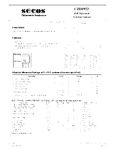
                                                                                                           CZD1952
                                                                                                             PNP High Speed
                     Elektronische Bauelemente
                                                                                                          Switching Transistor

                                                                RoHS Compliant Product
                                                                                                                         TO-252


    Description
    The CZD1952 is designed for high speed switching applications.


    Features
    *   Wide SOA
    *   Low Saturation Voltage,Typically VCE(sat)=-0.2V at IC/IB=-3A/-0.15A
    *   High Speed Switching,Typically tf=-0.15us at IC=-3A
    *   Complements to CZD5103


                                                                                                          Millimeter                        Millimeter
                                                                                              REF.                           REF.
                                                                                                       Min.       Max.                    Min.      Max.
                                                                                               A       6.40       6.80         G          0.50      0.70
                                                                                               B       5.20       5.50         H          2.20      2.40
                                                                                               C       6.80       7.20         J          0.45      0.55
                                                                                               D       2.20       2.80         K            0       0.15
                                                                                               E         2.30 REF.             L          0.90      1.50
                                                                                               F       0.70       0.90         M          5.40      5.80
                                                                                               S       0.60       0.90         R          0.80      1.20

                                                                o
    Absolute Maximum Ratings at TA=25 C (unless otherwise specified)
                                  Parameter                                       Symbol                       Ratings                                  Unit
        Collector to Base Voltage                                                 VCBO                          -100                                      V

        Collector to Emitter Voltage                                               VCEO                          -60                                      V
        Emitter to Base Voltage                                                    VE BO                          -5
                                                                                                                   .                                      V
        Collect Current (DC)                                                       IC                            -5                                       A
        Collect Current (Pulse)                                                IC                               - 10                                      A
                                                                                     o
                                                                          PD (TA =25 C )                           1                                      W
        Total Power Dissipation                                                      o
                                                                          PD (TC =25 C )                          10                                      W
                                                                                                                                                          o
        Operating Junction and Storage Temperature Range                    Tj, Tstg                           -55~+150                                   C


  ELECTRICAL CHARACTERISTICS ( Tamp.=25 C unless otherwise specified)
                                                                      O


                  Parameter                             Symbol            Min.          Typ. Max.      Unit                    Test Cond itions
   Collector-Base Breakdown Voltage                       BVCBO           -100           -         -    V              IC=-50 uA, IE=0
   Collector-Emitter Breakdown Voltage                    BV CEO          -60            -         -    V              IC= - 1mA, IB=0
   Emitter-Base Breakdown Voltage                         BVEBO            -5            -         -    V              IE= - 50uA, IC=0
   Cut-off Current                                          ICES            -            -      - 10    uA             VCE=-100V, V EB=0
   Emitter Cut-off Current                                  IEBO            -            -      -10     uA             VEB=-5V, IC=0
                                                         *VCE(sat)1         -            -     -0.3     V              IC= -3A, IB= -0.15A
   Collector-Emitter Saturation Voltage
                                                         *VCE(sat)2         -            -     -0.5     V               IC= -4A, IB= -0.2A
                                                          *VBE(on)1           -          -     -1.2      V              IC= -3A, IB= -0.15A
   Base-Emitter Voltage, On
                                                          *VBE(on)2           -          -     -1.5      V              IC= -4A, IB= -0.2A
   DC Current Gain                                         *hFE1          120            -      320                     VCE=-2V, IC=-1A
   DC Current Gain                                         *hFE2          40             -       -                      VCE=-2V, IC= -3A
   Output Capacitance                                       Cob            -            130       -      pF             VCB=-10V,IE=0,f=1MHz
   Transition Frequency                                       fT           -            80         -    MHz             VCE=- 10V, IE=0.5A,f=30MHz
   Turn-On Time                                              ton           -              -      0.3                     IC=-3A,RL=10


◦ Jabse Service Manual Search 2024 ◦ Jabse PravopisonTap.bg ◦ Other service manual resources online : FixyaeServiceinfo