Service Manuals, User Guides, Schematic Diagrams or docs for : . Electronic Components Datasheets Active components Transistors Secos sjv01n60

<< Back | Home

Most service manuals and schematics are PDF files, so You will need Adobre Acrobat Reader to view : Acrobat Download Some of the files are DjVu format. Readers and resources available here : DjVu Resources
For the compressed files, most common are zip and rar. Please, extract files with Your favorite compression software ( WinZip, WinRAR ... ) before viewing. If a document has multiple parts, You should download all, before extracting.
Good luck. Repair on Your own risk. Make sure You know what You are doing.


Image preview - the first page of the document
sjv01n60


>> Download sjv01n60 documenatation <<

Text preview - extract from the document
                                                                                                  SJV01N60
                                                                                        1A , 600V , RDS(ON) 10 m
                     Elektronische Bauelemente                                N-Channel Enhancement Mode Power MOSFET

                                                          RoHS Compliant Product
                                                A suffix of "-C" specifies halogen & lead-free
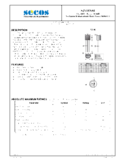


 DESCRIPTION                                                                                                          TO-92
         The high voltage MOSFET uses an advanced
                                                                                                                  A              D
   termination scheme to provide enhanced voltage-blocking
   capability without degrading performance over time. In addition,                                                     B
   this advanced MOSFET is designed to withstand high energy
   in avalanche and commutation modes . The new energy
   efficient design also offers a drain-to-source diode with a
                                                                                                        E               C        F
   fast recovery time. Designed for high voltage, high speed
   switching applications in power suppliers, converters and
   PWM motor controls ,these devices are particularly well
                                                                                                        G
   suited for bridge circuits where diode speed and commutating                                                          H
                                                                                                                                 1 Gate
   safe operating areas are critical and offer additional and safety                                                             2 Drain
   margin against unexpected voltage transients.                                                                         J
                                                                                                                                 3 Source


                                                                                                               Millimeter                  Millimeter
 FEATURES                                                                                        REF.
                                                                                                             Min.     Max.
                                                                                                                                 REF.
                                                                                                                                         Min.     Max.
                                                                                                  A          4.40     4.70           F   0.30     0.51
         Robust High Voltage Termination                                                          B          4.30     4.70           G     1.27 TYP.
                                                                                                  C          12.70      -            H   1.10     1.40
         Avalanche Energy Specified                                                               D          3.30     3.81           J   2.42     2.66
         Source-to-Drain Diode Recovery Time                                                      E          0.36     0.56           K   0.36     0.76

         Comparable to a Discrete Fast Recovery Diode
                                                                                                                             D
         Diode is Characterized for Use in Bridge Circuits
                                                                                                                             2
         IDSS and VDS(on) Specified at Elevated Temperature

                                                                                                             1
                                                                                                              G

                                                                                                                             3
                                                                                                                             S


 ABSOLUTE MAXIMUM RATINGS (TA=25


◦ Jabse Service Manual Search 2024 ◦ Jabse PravopisonTap.bg ◦ Other service manual resources online : FixyaeServiceinfo