Service Manuals, User Guides, Schematic Diagrams or docs for : . Electronic Components Datasheets Active components Transistors Secos pzt2222a

<< Back | Home

Most service manuals and schematics are PDF files, so You will need Adobre Acrobat Reader to view : Acrobat Download Some of the files are DjVu format. Readers and resources available here : DjVu Resources
For the compressed files, most common are zip and rar. Please, extract files with Your favorite compression software ( WinZip, WinRAR ... ) before viewing. If a document has multiple parts, You should download all, before extracting.
Good luck. Repair on Your own risk. Make sure You know what You are doing.


Image preview - the first page of the document
pzt2222a


>> Download pzt2222a documenatation <<

Text preview - extract from the document
                                                                                                    PZT2222A
                                                                                                         NPN Silicon
                     Elektronische Bauelemente                                                     General Purpose Transistor

                                                            RoHS Compliant Product
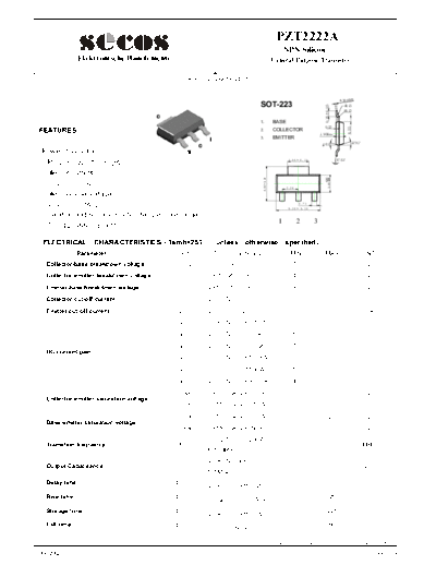


                                                                                              SOT-223
                                            C
                                                                                              1.   BASE
  FEATURES                                                                                    2.   COLLECTOR

                                                                    E                         3.   EMITTER
                                                                C
   Power dissipation                                        B
    P CM : 1 W Tamb=25
   Collector current
     I CM : 0.6 A
   Collector-base voltage
    V (BR)CBO : 75 V
   Operating and storage junction temperature range
                                                                                                     1        2         3
    T J Tstg: -55 to +150                                                                                                            Unit : mm


    ELECTRICAL CHARACTERISTICS                  Tamb=25                 unless        otherwise          specified
                  Parameter                       Symbol              Test        conditions               MIN                MAX                 UNIT
     Collector-base breakdown voltage            V(BR)CBO           Ic= 10    A        IE=0                  75                                     V
     Collector-emitter breakdown voltage         V(BR)CEO           Ic= 10mA         IB=0                    40                                     V
     Emitter-base breakdown voltage              V(BR)EBO           IE=10     A      IC=0                    6                                      V
     Collector cut-off current                     ICBO             VCB=60V ,       IE=0                                      0. 01                   A
     Emitter cut-off current                       IEBO             VEB= 3V ,        IC=0                                     0. 01                   A
                                                   hFE(1)           VCE=10V,       IC= 0.1mA                 35
                                                   hFE(2)           VCE=10V,       IC= 1mA                   50
                                                   hFE(3)           VCE=10V,       IC= 10mA                  75
     DC current gain
                                                   hFE(4)           VCE=10V,       IC= 150mA                100                300
                                                   hFE(5)           VCE=1V,       IC= 150mA                  50
                                                   hFE(6)           VCE=10V,       IC= 500mA                 40
                                                 VCE(sat)           IC=500 mA, IB= 50mA                                          1                  V
     Collector-emitter saturation voltage
                                                 VCE(sat)           IC=150 mA, IB= 15mA                                         0.3                 V
                                                 VBE(sat)           IC=500 mA, IB= 50mA                                         2.0                 V
     Base-emitter saturation voltage
                                                 VBE(sat)           IC=150 mA, IB=15mA                      0.6                 1.2                 V
                                                                    VCE=20V,       IC= 20mA
     Transition frequency                              fT                                                   300                                   MHz
                                                                    f=100MHz
                                                                    VCB=10V,       I E= 0
     Output Capacitance                          Cob                                                                             8                  pF
                                                                    f=1MHz
     Delay time                                   td                VCC=30V, IC=150mA
                                                                                                                                10                 nS

     Rise time                                    tr                VBE(off)=0.5V,IB1=15mA
                                                                                                                                25                 nS

     Storage time                                 tS                VCC=30V, IC=150mA
                                                                                                                               225                 nS

     Fall time                                    tf                IB1= IB2= 15mA
                                                                                                                                60                 nS

  http://www.SeCoSGmbH.com                                                                           Any changing of specification will not be informed individual

01-Jun-2002 Rev. A                                                                                                                                       Page 1 of 4
                                                                                                                                                           PZT2222A
                                                                                                                                                                NPN Silicon
                                                    Elektronische Bauelemente                                                                        General Purpose Transistor


   SWITCHING TIME EQUIVALENT TEST CIRCUITS


                                                                                                   +30 V                                                                              +30 V
                                                                     1.0 to 100 s,                                                                1.0 to 100 s,                        200
                                                                                                   200                           +16 V
                                              +16 V                  DUTY CYCLE  2.0%                                                             DUTY CYCLE  2.0%

                                      0                                                                                            0
                                                                                  1 k                                                  -14 V                         1k                       CS* < 10 pF
                                     -2 V                                                                  CS* < 10 pF
                                                            < 2 ns                                                                                  < 20 ns
                                                                                                                                                                     1N914

                                                                                                            Scope rise time < 4 ns                                           -4 V
                                                                                                            *Total shunt capacitance of test jig,
                                                                                                            connectors, and oscilloscope.
                                                             Figure 1. Turn


◦ Jabse Service Manual Search 2024 ◦ Jabse PravopisonTap.bg ◦ Other service manual resources online : FixyaeServiceinfo