Service Manuals, User Guides, Schematic Diagrams or docs for : . Electronic Components Datasheets Active components Transistors Secos pzt359

<< Back | Home

Most service manuals and schematics are PDF files, so You will need Adobre Acrobat Reader to view : Acrobat Download Some of the files are DjVu format. Readers and resources available here : DjVu Resources
For the compressed files, most common are zip and rar. Please, extract files with Your favorite compression software ( WinZip, WinRAR ... ) before viewing. If a document has multiple parts, You should download all, before extracting.
Good luck. Repair on Your own risk. Make sure You know what You are doing.


Image preview - the first page of the document
pzt359


>> Download pzt359 documenatation <<

Text preview - extract from the document
                                                                                                               PZT359
                                                                                                          PNP Silicon Planar
                     Elektronische Bauelemente                                                           High Current Transistor
                                                                      RoHS Compliant Product


    Features
      5 Amps continuous current, up to 10 Amp peak current.                                                              SOT-223
       Excellent gain characteristic specified up to 10Amps.
      Very low saturation voltage
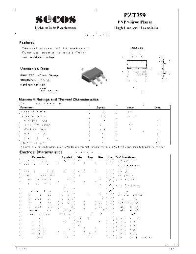


     Mechanical Data                                              C

     Case: SOT-223 Plastic Package
                                                                                                                                                                 1.6

     Weight: approx. 0.021g                                                                    E
                                                                                                                   1         2        3
                                                                                      C
     Marking Code: 359                                                          B
                   xxxx                                                                                             1.   BASE
                          (xxxx = date code)                                                                        2.   COLLECTOR
                                                                                                                    3.   EMITTER

    Maximum Ratings and Thermal Characteristics
     (TA = 25OC, unless otherwise noted)
     Parameter                                                                  Symbol                            Value                            Unit
                                                                                                                                                    O
     Junction Temperature                                                                 Tj                       +150                                 C
                                                                                                                                                    O
     Storage Temperature                                                              Tstg                     -55 to +150                              C
     Collector-Base Voltage                                                          VCBO                          -140                              V
     Collector-Emitter Voltage                                                       VCEO                          -100                              V
     Emitter-Base Voltage                                                            V EBO                           -6                              V
     Collector Current (DC)                                                               IC                         -5                              A
     Collector Current (Pulse)                                                            IC                        -10                              A
     Total Power Dissipation                                                              PD                         3                              W
    *The power which can be dissipated assuming the device is mounted in a typical manner on a P.C.B. with copper equal to 4 square inch minimum.

    Electrical Characteristics (TJ = 25 C, unless otherwise noted)
                                                         O


                Parameter                       Symbol        Min       Typ.        Max            Uni   Test Conditions
       Collector-Base Breakdown Voltage         BVCBO        -140        -           -              V    I C=-100A, I E=0
      Collector-Emitter Breakdown Voltage
               (w/ Real Device Limit)
                                                BVCER        -140         -           -            V     I C=-1A, R B<=1K

      Collector-Emitter Breakdown Voltage       *BVCEO       -100         -          -              V    I C=-10mA, I B=0
        Emitter-Base Breakdown Voltage           BVEBO        -6          -          -              V    I E=-100A, IC=0
         Collector-Base Cutoff Current            I CBO        -          -         -50            nA    VCB=-100V, IE=0
         Collector-Base Cutoff Current
               (w/ Real Device Limit)
                                                 I CER        -           -         -50            nA    VCB=-100V, R<=1K

          Emitter-Base Cutoff Current              I EBO      -            -         -10           nA  VEB=-6V, IC=0
         Collector Saturation Voltage 1        *VCE(sat)1     -          -20         -50           mV  I C=-100mA, I B=-10mA
         Collector Saturation Voltage 2        *VCE(sat)2     -          -90        -115           mV  I C=-1A, I B=-100mA
         Collector Saturation Voltage 3        *VCE(sat)3     -         -160        -220           mV  I C=-2A, I B=-200mA
         Collector Saturation Voltage 4        *VCE(sat)4     -         -300        -420           mV  I C=-4A, I B=-400mA
            Base Saturation Voltage             *VBE(sat)     -         -1.01       -1.17           V  I C=-4A, I B=-400mA
             Base-Emitter Voltage               *VBE(on)      -        -0.925       -1.16           V  VCE=-1V, I C=-4A
              DC Current Gain 1                   *hFE1      100         200          -                VCE=-1V, I C=-10mA
              DC Current Gain 2                   *hFE2      100         200         300               VCE=-1V, I C=-1A
              DC Current Gain 3                   *hFE3      50           90          -                VCE=-1V, I C=-3A
              DC Current Gain 4                   *hFE4      30           50          -                VCE=-1V, I C=-4A
              DC Current Gain 5                   *hFE5       -           15          -                VCE=-1V, I C=-10A
            Gain-Bandwidth Product                   fT       -          125          -            MHz VCE=-10V, IC=-100mA, f=50MHz

  http://www.SeCoSGmbH.com                                                                                      Any changing of specification will not be informed individual
01-Jun-2002 Rev. A                                                                                                                                               Page 1 of 2
                                                                                         PZT359
                                                                                     PNP Silicon Planar
                     Elektronische Bauelemente
                                                                                 High Current Transistor

              Output Capacitance               Cob          -       65      -   pF   VCB=-10V, IE=0, f=1MHz
                     O n-Time                   ton         -      110      -
                                                                                ns   VCC=-10V, IC=2A, I B1=-200mA,I B1=200mA
                     Off-Time                  toff         -      460      -
       *Measured under pulse condition. Pulse width    300 s, Duty Cycle   2%
        Spice parameter data is available upon request for this device.


 http://www.SeCoSGmbH.com                                                                Any changing of specification will not be informed individual

01-Jun-2002 Rev. A                                                                                                                          Page 2 of 2


◦ Jabse Service Manual Search 2024 ◦ Jabse PravopisonTap.bg ◦ Other service manual resources online : FixyaeServiceinfo